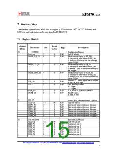
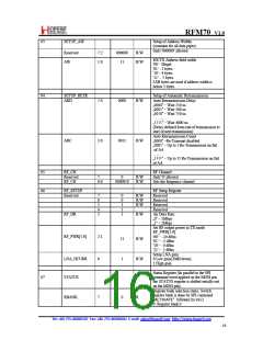
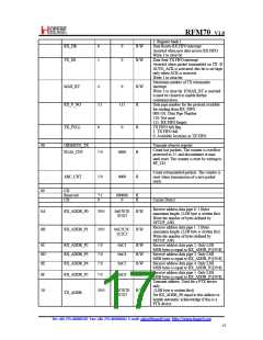
RFM70 V1.0
This write command followed by data 0x73 activates
the following features:
• R_RX_P
L
_
W
ID
•• W
_
_
ACK_P
A
YL
O
A
AD
W
T
X
_P
A
YL
O
D_NOACK
A new ACTIVATE command with the same data
deactivates them again. This is executable in power
down or stand by modes only.
The R_RX_PL_WID, W_ACK_PAYLOAD, and
W_TX_PAYLOAD_NOACK features registers are
initially in a deactivated state; a write has no effect, a
read only results in zeros on MISO. To activate these
registers, use the ACTIVATE command followed by
data 0x73. Then they can be accessed as any other
register. Use the same command and data to
deactivate the registers again.
ACTIVATE
0101 0000
1
This write command followed by data 0x53 toggles
the register bank, and the current register bank
number can be read out from REG7 [7]
Read RX-payload width for the top
R_RX_PL_WID
0110 0000
1010 1PPP
R_RX_PAYLOAD in the RX FIFO.
Used in RX mode.
Write Payload to be transmitted together with
ACK packet on PIPE PPP. (PPP valid in the range
from 000 to 101). Maximum three ACK packet
payloads can be pending. Payloads with same PPP are
handled using first in - first out principle. Write
1 to 32
LSB byte first
W_ACK_PAYLOAD
payload: 1– 32 bytes. A write operation always starts
at byte 0.
Used in TX mode. Disables AUTOACK on this
specific packet.
W_TX_PAYLOAD_NO
ACK
1 to 32
LSB byte first
1011 0000
1111 1111
No Operation. Might be used to read the STATUS
register
NOP
0
Table 2 SPI command
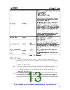
6.3.2 SPI Timing
SCK
CSN
Write to SPI register:
MOSI
MISO
x
x
x
C7 C6 C5 C4 C3 C2 C1
S7 S6 S5 S4 S3 S2 S1
C0
S0
D7 D6
0
D5 D4
D3 D2
D1 D0
HI-Z
Hi-Z
0
0
0
0
0
0
0
Read from SPI register:
x
C7 C6 C5 C4 C3 C2 C1
C0
S0
x
MOSI
MISO
x
x
S7 S6 S5 S4 S3 S2 S1
D7
D6
D5 D4
D3 D2
D1 D0
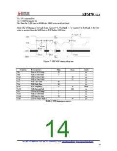
Figure 6 SPI timing
Tel: +86‐755‐86096587 Fax: +86‐755‐86096602 E‐mail: sales@hoperf.com http://www.hoperf.com
13

 HOPERF [ HOPERF ]