HT46R01A
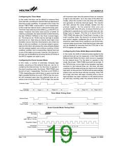
Port A Wake-up
the pin is setup as an external interrupt input the I/O
function still remains.
If the HALT instruction is executed, the device will enter
the Power Down Mode, where the system clock will stop
resulting in power being conserved, a feature that is im-
portant for battery and other low-power applications.
Various methods exist to wake-up the microcontroller,
one of which is to change the logic condition on one of
the PA0~PA7 pins from high to low. After a HALT instruc-
tion forces the microcontroller into entering the Power
Down Mode, the processor will remain idle or in a
low-power state until the logic condition of the selected
wake-up pin on Port A changes from high to low. This
function is especially suitable for applications that can
be woken up via external switches. Note that pins PA0 to
PA7 can be selected individually to have this wake-up
feature using an internal register known as PAWK, lo-
cated in the Data Memory.
·
External Timer/Event Counter Input
The device contains a single Timer/Event Counter.
The Timer/Event Counter has an external input pin,
known as TMR0 which is pin-shared with the I/O pin
PA2. For the shared pin to be used as a Timer/Event
Counter input, the Timer/Event Counter must be con-
figured to be in the Event Counter or Pulse Width
Measurement Mode. This is achieved by setting the
appropriate bits in the Timer/Event Counter Control
Register. The pin must also be setup as an input by
setting the appropriate bit in the Port Control Register.
Pull-high resistor options can also be selected via the
port pull-high resistor register. Note that even if the pin
is setup as an external timer input the I/O function still
remains.
·
PFD Output
The device contains a PFD function whose single out-
put is pin-shared with PA1. The PFD output function of
this pin along with the timer source is chosen via bits
in the CTRL0 register. Note that the corresponding bit
of the port control register, PAC.1, must setup the pin
as an output to enable the PFD output. If the PAC port
control register has setup the pin as an input, then the
pin will function as a normal logic input with the usual
pull-high option, even if the PFD has been selected.
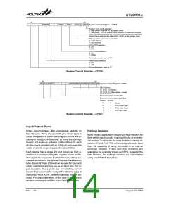
I/O Port Control Registers
Port A has its own control register, known as PAC, which
controls the input/output configuration. With this control
register, each PA0~PA6 I/O pin with or without pull-high
resistors can be reconfigured dynamically under soft-
ware control. Pins PA0 to PA6 port are directly mapped
to a bit in its associated port control register. For the I/O
pin to function as an input, the corresponding bit of the
control register must be written as a ²1². This will then
allow the logic state of the input pin to be directly read by
instructions. When the corresponding bit of the control
register is written as a ²0², the I/O pin will be setup as a
CMOS output. If the pin is currently setup as an output,
instructions can still be used to read the output register.
However, it should be noted that the program will in fact
only read the status of the output data latch and not the
actual logic status of the output pin.
·
PWM Output
The device contains a single PWM output pin shared
with pins PA4. The PWM output function of this pin
along with the mode type is chosen via bits in the
CTRL0 register. Note that the corresponding bit or bits
of the port control register, PAC.4, must setup the pin
as an output to enable the PWM output. If the PAC
port control register has setup the pin as an input, then
the pin will function as a normal logic input with the
usual pull-high resistor option, even if the PWM has
been selected.
Pin-shared Functions
·
A/D Inputs
The device has four A/D converter inputs. All of these
analog inputs are pin-shared with PA0 to PA3. If these
pins are to be used as A/D inputs and not as normal
I/O pins then the corresponding bits in the A/D Con-
verter Control Register, ADCR, must be properly set.
There are no configuration options associated with
the A/D function. If used as I/O pins, then full pull-high
resistor selections remain, however if used as A/D in-
puts then any pull-high resistor selections associated
with these pins will be automatically disconnected.
The flexibility of the microcontroller range is greatly en-
hanced by the use of pins that have more than one func-
tion. Limited numbers of pins can force serious design
constraints on designers but by supplying pins with
multi-functions, many of these difficulties can be over-
come. For some pins, the chosen function of the
multi-function I/O pins is set by configuration options
while for others the function is set by application pro-
gram control.
·
External Interrupt Input
I/O Pin Structures
The external interrupt pin, INT, is pin-shared with the
I/O pin PA3. To use the pin as an external interrupt in-
put the correct bits in the INTCO register must be pro-
grammed. The pin must also be setup as an input by
setting the appropriate bit in the Port Control Register.
A pull-high resistor can also be selected via the appro-
priate port pull-high resistor register. Note that even if
The diagrams illustrate the I/O pin internal structures. As
the exact logical construction of the I/O pin may differ
from these drawings, they are supplied as a guide only
to assist with the functional understanding of the I/O
pins.
Rev. 1.10
15
August 13, 2008

 HOLTIC [ HOLT INTEGRATED CIRCUITS ]