HT46R01A
b
7
b
0
P
W
M
S
E
L
P
W
M
C
P
F
D
C
Q
O
S
C
C
L
K
M
O
D
S
y
s
t
e
m
C
o
n
t
r
o
l
R
e
g
i
s
t
e
r
C
T
R
L
0
S
0
y
s
t
e
m
c
l
o
e
c
k
m
o
d
e
s
e
l
e
c
t
i
o
n
:
:
h
i
g
h
s
p
e
d
-
I
n
t
e
r
n
a
l
R
C
a
s
s
y
s
t
e
m
c
l
o
c
k
1
l
o
w
s
p
e
e
d
-
R
T
C
a
s
s
y
s
t
e
m
c
l
o
c
k
,
I
n
t
e
r
n
a
l
R
C
o
s
c
i
l
l
a
t
o
r
s
t
o
p
p
e
d
N
o
t
e
t
h
a
t
t
h
e
s
e
s
e
l
e
c
t
i
o
n
s
a
r
e
o
n
l
y
v
a
l
i
d
i
f
t
h
e
o
s
c
i
l
l
a
t
o
r
c
o
n
f
i
g
u
r
a
t
i
o
n
o
p
t
i
o
n
s
h
a
v
e
s
e
l
e
c
t
e
d
t
a
h
e
I
n
t
e
r
n
a
l
t
R
o
C
+
R
T
C
a
s
t
h
e
s
y
s
t
e
m
c
l
o
c
k
R
0
1
T
C
o
s
c
i
l
l
a
t
o
r
q
u
i
c
k
s
t
r
t
-
u
p
f
u
n
c
i
n
:
q
s
u
i
c
k
s
t
a
r
t
-
u
p
:
l
o
w
s
t
a
r
t
-
u
p
I
0
1
/
O
:
:
o
r
P
F
D
s
e
l
e
c
t
i
o
n
I
P
/
O
F
D
I
0
1
/
O
:
:
o
r
P
W
M
s
e
l
e
c
t
i
o
n
I
P
/
O
W
M
N
o
t
i
m
p
l
e
m
e
n
t
e
d
,
r
i
e
a
d
a
s
"
0
"
P
W
M
m
o
d
e
s
e
l
e
c
t
o
n
0
1
:
:
6
7
+
+
2
1
N
o
t
i
m
p
l
e
m
e
n
t
e
d
,
r
e
a
d
a
s
"
0
"
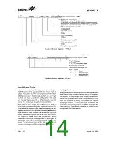
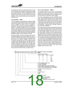
System Control Register - CTRL0
b
7
b
0
I
N
T
E
S
1
I
N
T
E
S
0
W
D
T
E
N
3
W
D
T
E
N
2
W
D
T
E
N
1
W
D
T
E
N
0
S
y
s
t
e
m
C
o
n
t
r
o
l
R
e
g
i
s
t
e
r
C
T
R
L
1
W
D
T
f
u
n
c
t
i
o
n
1
0
1
0
d
i
s
a
b
l
e
X
X
X
X
o
t
h
e
r
v
a
l
u
e
s
-
e
n
a
b
l
e
N
o
t
i
m
p
l
e
m
e
n
t
E
e
d
,
r
e
a
d
a
s
"
0
"
E
x
t
e
r
n
a
l
i
n
t
e
r
r
u
p
t
e
d
g
e
t
r
i
g
g
e
r
t
y
p
e
I
N
T
E
S
1
I
N
T
S
0
0
0
1
1
0
1
0
1
d
i
s
s
a
b
g
l
e
r
i
i
l
n
i
e
d
g
e
t
r
i
g
i
g
e
r
f
d
a
l
n
g
e
d
g
e
t
r
g
g
e
r
u
a
l
e
d
g
e
t
r
i
g
g
e
r
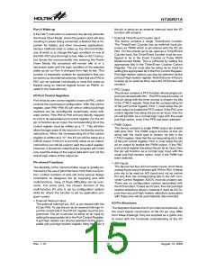
System Control Register - CTRL1
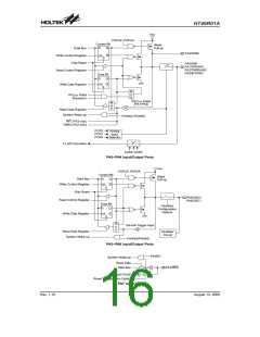
Input/Output Ports
Holtek microcontrollers offer considerable flexibility on
their I/O ports. There are seven I/O pins whose input or
output designation is under user program control and an
additional input pin. Additionally, as there are pull-high
resistor and wake-up software configurations for each
pin, the user is provided with an I/O structure to meet the
needs of a wide range of application possibilities.
Pull-high Resistors
Many product applications require pull-high resistors for
their switch inputs usually requiring the use of an exter-
nal resistor. To eliminate the need for these external re-
sistors, I/O pins PA0~PA6, when configured as an input
have the capability of being connected to an internal
pull-high resistor. These pull-high resistors are
selectable via a register known as PAPU, located in the
Data Memory. The pull-high resistors are implemented
using weak PMOS transistors.
Each device has a single I/O port known as Port A,
which has a corresponding data register known as PA.
This register is mapped to the Data Memory with an ad-
dresses as shown in the Special Purpose Data Memory
table. Seven of these I/O lines can be used for input and
output operations and one line as an input only. For in-
put operation, these ports are non-latching, which
means the inputs must be ready at the T2 rising edge of
instruction ²MOV A,[m]², where m denotes the port ad-
dress. For output operation, all the data is latched and
remains unchanged until the output latch is rewritten.
Rev. 1.10
14
August 13, 2008

 HOLTIC [ HOLT INTEGRATED CIRCUITS ]