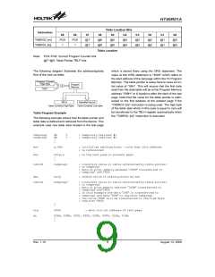
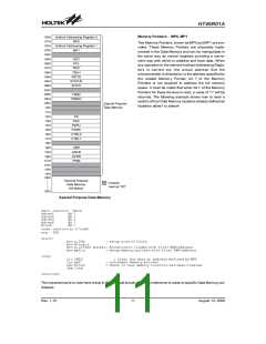
HT46R01A
In addition, on entering an interrupt sequence or execut-
ing a subroutine call, the status register will not be
pushed onto the stack automatically. If the contents of
the status registers are important and if the interrupt rou-
tine can change the status register, precautions must be
taken to correctly save it.
Pulse Width Modulation Register - PWM
Each device contains a Pulse Width Modulator which
has a corresponding control register, known as PWM.
The 8-bit contents of this register defines the duty cycle
value for the modulation cycle of the Pulse Width Modu-
lator.
Interrupt Control Registers - INTC0
A/D Converter Register - ADR, ADCR, ACSR
The 8-bit register, known as INTC0, control the opera-
tion of both external, and internal timer and A/D inter-
rupts. By setting various bits within this register using
standard bit manipulation instructions, the enable/dis-
able function of each interrupt can be independently
controlled. A master interrupt bit within this register, the
EMI bit, acts like a global enable/disable and is used to
set all of the interrupt enable bits on or off. This bit is
cleared when an interrupt routine is entered to disable
further interrupt and is set by executing the ²RETI² in-
struction.
The device contains a 4-channel 8-bit A/D converter,
which has a single data register, known as ADR. This is
the register where the digital value is placed after the
completion of an analog to digital conversion cycle. The
channel selection and configuration of the A/D converter
is setup via the control register ADCR while the A/D
clock frequency is defined by the clock source register,
ACSR.
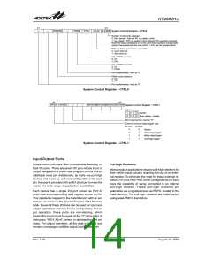
System Control Register - CTRL0
This register is used to provide control over certain inter-
nal functions including certain system clock options, the
PFD clock source and on/off control, the PWM mode
and on/off control and an RTC Oscillator quick start up
function.
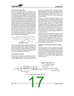
Timer/Event Counter Registers
Depending upon which device is selected, all devices
contain one or two integrated 8-bit Timer/Event Coun-
ters. For the device, which have a single 8-bit Timer/
Event Counter, an associated register known as TMR0
is the location where the timer¢s 8-bit value is located.
An associated control register, known as TMR0C, con-
tains the setup information for this timer.
System Control Register - CTRL1
This register is used to provide control over certain inter-
nal functions including the External Interrupt edge trig-
ger type and the Watchdog Timer control function.
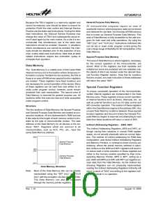
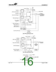
Input/Output Ports and Control Registers
Wake-up Function Register - PAWK
Within the area of Special Function Registers, the port
PA data I/O register and its associated control register
PAC play a prominent role. These registers are mapped
to specific addresses within the Data Memory as shown
in the Data Memory table. The PA data I/O register, is
used to transfer the appropriate output or input data on
the PA port. The PAC control register specifies which
pins of PA are set as inputs and which are set as out-
puts. To setup a pin as an input, the corresponding bit of
the control register must be set high, for an output it
must be set low. During program initialisation, it is impor-
tant to first setup the control registers to specify which
pins are outputs and which are inputs before reading
data from or writing data to the I/O ports. One flexible
feature of these registers is the ability to directly pro-
gram single bits using the ²SET [m].i² and ²CLR [m].i²
instructions. The ability to change I/O pins from output to
input and vice versa by manipulating specific bits of the
I/O control registers during normal program operation is
a useful feature of these devices.
When the microcontroller enters the Power Down Mode,
various methods exist to wake the device up and con-
tinue with normal operation. One method is to allow a
low going edge on the I/O pins to have a wake-up func-
tion. This register is used to select which I/O pins are
used to have this wake-up function.
Pull-high Register - PAPU
The I/O pins, if configured as inputs, can have internal
pull-high resistors connected, which eliminates the need
for external pull-high resistors. This register selects which
I/O pins are connected to internal pull-high resistors.
Rev. 1.10
13
August 13, 2008

 HOLTIC [ HOLT INTEGRATED CIRCUITS ]