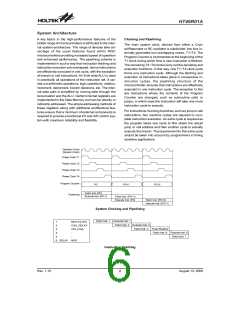
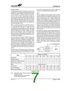
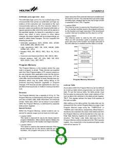
HT46R01A
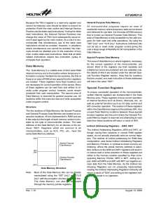
General Purpose Data Memory
Because the TBLH register is a read-only register and
cannot be restored, care should be taken to ensure its
protection if both the main routine and Interrupt Service
Routine use the table read instructions. If using the table
read instructions, the Interrupt Service Routines may
change the value of TBLH and subsequently cause er-
rors if used again by the main routine. As a rule it is rec-
ommended that simultaneous use of the table read
instructions should be avoided. However, in situations
where simultaneous use cannot be avoided, the inter-
rupts should be disabled prior to the execution of any
main routine table-read instructions. Note that all table
related instructions require two instruction cycles to
complete their operation.
All microcontroller programs require an area of
read/write memory where temporary data can be stored
and retrieved for use later. It is this area of RAM memory
that is known as General Purpose Data Memory. This
area of Data Memory is fully accessible by the user pro-
gram for both read and write operations. By using the
²SET [m].i² and ²CLR [m].i² instructions individual bits
can be set or reset under program control giving the
user a large range of flexibility for bit manipulation in the
Data Memory.
Special Purpose Data Memory
This area of Data Memory is where registers, necessary
for the correct operation of the microcontroller, are
stored. Most of the registers are both readable and
writable but some are protected and are readable only,
the details of which are located under the relevant Spe-
cial Function Register section. Note that for locations
that are unused, any read instruction to these addresses
will return the value ²00H².
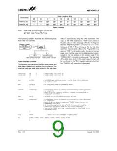
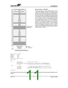
Data Memory
The Data Memory is a volatile area of 8-bit wide RAM
internal memory and is the location where temporary in-
formation is stored. Divided into two sections, the first of
these is an area of RAM where special function registers
are located. These registers have fixed locations and
are necessary for correct operation of the device. Many
of these registers can be read from and written to di-
rectly under program control, however, some remain
protected from user manipulation. The second area of
Data Memory is reserved for general purpose use. All
locations within this area are read and write accessible
under program control.
Special Function Registers
To ensure successful operation of the microcontroller,
certain internal registers are implemented in the Data
Memory area. These registers ensure correct operation
of internal functions such as timers, interrupts, etc., as
well as external functions such as I/O data control and
A/D converter operation. The location of these registers
within the Data Memory begins at the address 00H. Any
unused Data Memory locations between these special
function registers and the point where the General Pur-
pose Memory begins is reserved and attempting to read
data from these locations will return a value of 00H.
Structure
The two sections of Data Memory, the Special Purpose
and General Purpose Data Memory are located at con-
secutive locations. All are implemented in RAM and are
8 bits wide but the length of each memory section is dic-
tated by the type of microcontroller chosen. The start
address of the Data Memory for all devices is the ad-
dress ²00H². Registers which are common to all
microcontrollers, such as ACC, PCL, etc., have the
same Data Memory address.
Indirect Addressing Registers - IAR0, IAR1
The Indirect Addressing Registers, IAR0 and IAR1, al-
though having their locations in normal RAM register
space, do not actually physically exist as normal regis-
ters. The method of indirect addressing for RAM data
manipulation uses these Indirect Addressing Registers
and Memory Pointers, in contrast to direct memory ad-
dressing, where the actual memory address is speci-
fied. Actions on the IAR0 and IAR1 registers will result in
no actual read or write operation to these registers but
rather to the memory location specified by their corre-
sponding Memory Pointer, MP0 or MP1. Acting as a
pair, IAR0 with MP0 and IAR1 with MP1 can together ac-
cess data from the Data Memory. As the Indirect Ad-
dressing Registers are not physically implemented,
reading the Indirect Addressing Registers indirectly will
return a result of ²00H² and writing to the registers indi-
rectly will result in no operation.
0
0
H
S
D
p
e
c
i
a
l
P
u
r
p
o
s
e
a
t
a
M
e
m
o
r
y
1
F
H
2
0
H
G
D
e
n
e
r
a
l
P
u
r
p
o
s
e
a
t
a
M
e
m
o
r
y
5
F
H
Data Memory Structure
Note: Most of the Data Memory bits can be directly
manipulated using the ²SET [m].i² and ²CLR
[m].i² with the exception of a few dedicated bits.
The Data Memory can also be accessed
through the memory pointer registers.
Rev. 1.10
10
August 13, 2008

 HOLTIC [ HOLT INTEGRATED CIRCUITS ]