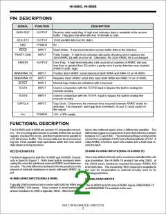
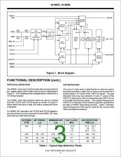
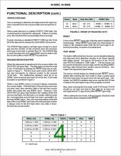
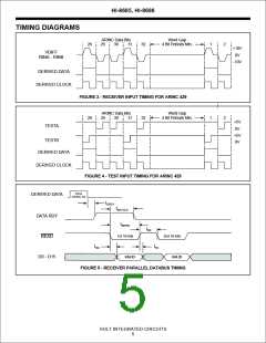
HI-8685, HI-8686
RECOMMENDED OPERATING CONDITIONS
ABSOLUTE MAXIMUM RATINGS
All voltages referenced to GND
Supply voltages
Supply Voltages
VCC ....................................................... +7.0V
VCC .................................................+5V ± 10%
Voltage on inputs
Temperature Range
RINA (-10) to RINB (-10) ......... +29V to - 29V
All other input pins..................-0.3 to Vcc +0.3
Industrial Screening .............. -40°C to +85°C
Hi-Temp Screening .............. -55°C to +125°C
Military Screening..................-55°C to +125°C
DC current per input pin ....................... +10mA
Junction Temperature, Tj .................... £+ 175°C
Power dissipation at 25°C
plastic 28-pin SO..... 1.8W, derate 14.1mW/°C
plastic 28-pin PLCC .2.3 W, derate 18.2mW/°C
plastic 32-pin SO......1.6 W, derate 15.4mW/°C
NOTE: Stresses above absolute maximum
ratings or outside recommended operating
conditions may cause permanent damage to
the device. These are stress ratings only.
Operation at the limits is not recommended.
Solder Temperature
Leads ............................. +280°C for 10 sec
Package body ..................................+220°C
Storage Temperature ............. -65°C to +150°C
DC ELECTRICAL CHARACTERISTICS
Vcc = 5V, GND = 0V, TA = Operating Temperature Range (unless otherwise specified).
PARAMETERS
SYMBOL TEST CONDITIONS
MIN TYP MAX UNITS
ARINC Bus Inputs (RINA, RINB, RINA-10 & RINB-10)
Differential input voltage
one or zero
null
common mode
VDIN
VNIN
VCOM
differential voltage
6.5
-
-
10.0 13.0
volts
"
"
"
"
-
-
2.75 volts
5.0
with respect to GND
volts
Input resistance
RINA (-10) to RINB(-10)
RINA (-10) or RINB(-10) to GND or VCC
RDIFF
RSUP
supplies floating
30
19
75
40
-
-
Kohm
Kohm
"
"
"
'
Input capacitance (Guaranteed but not tested)
differential
to GND
to VCC
CDIFF
CG
CH
RINA (-10) to RINB (-10)
-
-
-
-
-
-
20
20
20
pF
pF
pF
HOLT INTEGRATED CIRCUITS
6

 HOLTIC [ HOLT INTEGRATED CIRCUITS ]