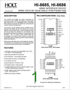
HI-8685, HI-8686
PIN DESCRIPTIONS
SIGNAL
FUNCTION
DESCRIPTION
DATA RDY
OUTPUT
Receiver data ready flag. A high level indicates data is available in the receive
buffer. Flag goes low when the first 16-bit byte is read.
D0 to D15
GND
OUTPUT
POWER
INPUT
16-bit parallel data bus (tri-state)
0V
READ
Read strobe. A low level transfers receive buffer data to the data bus
PARITY ENB
INPUT
Parity Enable - A high level activates odd parity checking which replaces the
32nd ARINC bit with an error bit. Otherwise, the 32nd ARINC bit is unchanged
ERROR
OUTPUT
Error Flag. A high level indicates a bit count error (number of ARINC bits was
less than or greater than 32) and/or a parity error if parity detection was enabled
(PARITY ENB high)
RINA/RINA-10
RINB/RINB-10
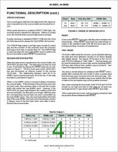
RESET
INPUT
INPUT
INPUT
INPUT
Positive direct ARINC serial data input (both RINA and RINA-10 on HI-8686)
Negative direct ARINC serial data input (both RINB and RINB-10 on HI-8686)
Internal logic states are initialized with a low level
TESTA
Used in conjunction with the TESTB input to bypass the built-in analog line
receiver circuitry
TESTB
INPUT
INPUT
U sed in conjunction with the TESTA input to bypass the built-in analog line
receiver circuitry
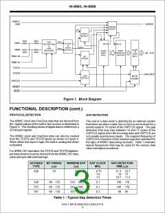
GAPCLK
Gap Clock. Determines the minimum time required between ARINC words for
detection. The minimum word gap time is between 16 and 17 clock cycles of
this signal.
Vcc
POWER
+5V ±10% supply
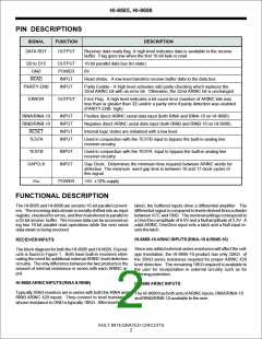
FUNCTIONAL DESCRIPTION
The HI-8685 and HI-8686 are serial to 16-bit parallel convert- lation, the buffered inputs drive a differential amplifier. The
ers. The incoming data stream is serially shifted into an input
register, checked for errors, and then transferred in parallel to
differential signal is compared to levels derived from a divider
between VCC and GND. The nominal settings correspond to
a 32-bit receive buffer. The receive data can be accessed us- a One/Zero amplitude of 6.0V and a Null amplitude of 3.3V. A
ing two 16-bit parallel read operations while the next serial valid ARINC One/Zero input sets a latch and a Null input re-
data steam is being received.
sets the latch.
HI-8685-10 ARINC INPUTS (RINA-10 & RINB-10)
Since any added external series resistance will affect the volt-
RECEIVER INPUTS
The block diagram for both the HI-8685 and HI-8685-10 prod-
ucts is found in Figure 1. Both have built-in receivers elimi- age translation, the HI-8685-10 product has only 25KW of
nating the need for additional external ARINC level detection
circuitry. The only difference between the two products is the
am ount of internal resistance in series with each ARINC in-
put.
the 35KWseries resistance required for proper ARINC 429
level detection. The remaining 10KWrequired is available to
the user for incorporation in externa l circuitry such as for
lightning protection.
HI-8685 ARINC INPUTS (RINA & RINB)
HI-8686 ARINC INPUTS
Typically 35KWresistors are in series with both the RINA and
RINB ARINC 429 inputs. They connect to level translators
whose resistance to GND is typically 10KW. After level trans-
The HI-8686 has both sets of ARINC inputs, RINA/RINA-10
and RINB/RINB-10 available to the user.
HOLT INTEGRATED CIRCUITS
2

 HOLTIC [ HOLT INTEGRATED CIRCUITS ]