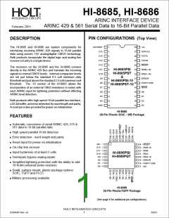
HI-8685, HI-8686
PARITY
ENB
ERROR
ERROR
DETECT
CLK
PARITY
DETECT
10KW
10KW
25KW
25KW
RXA
RXB
ESD
PROTECTION
&
LINE
RECEIVER
RINA
RINB
CLOCK
&
DATA
DETECT
BIT 32
BIT 32
DATA
32-BIT
TO
16-BIT
MUX
32-BIT
SHIFT
REG.
32-BIT
RECEIVE 32
BUFFER
32
16
D0 - D15
RINA-10
BIT
COUNT
RINB-10
TESTA
TESTB
DATA RDY
GAP
DETECT
BYTE
COUNT
GAPCLK
RESET
READ
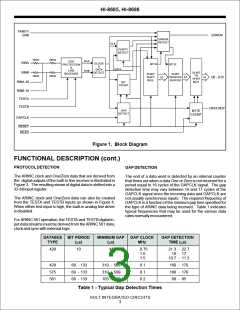
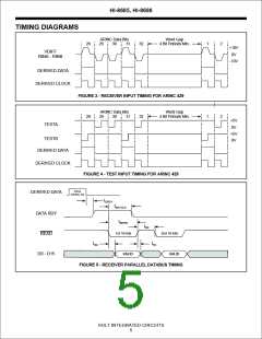
Figure 1. Block Diagram
FUNCTIONAL DESCRIPTION (cont.)
PROTOCOL DETECTION
GAP DETECTION
The ARINC clock and One/Zero data that are derived from
the digital outputs of the built-in line receiver is illustrated in
Figure 3. The resulting steam of digital data is shifted into a
32-bit input register.
The end of a data word is detected by an internal counter
that times out when a data One or Zero is not received for a
period equal to 16 cycles of the GAPCLK signal. The gap
detection time may vary between 16 and 17 cycles of the
GAPCLK signal since the incoming data and GAPCLK are
not usually synchronous inputs. The required frequency of
GAPCLK is a function of the mininum gap time specified for
the type of ARINC data being received. Table 1 indicates
typical frequencies that may be used for the various data
rates normally encountered.
The ARINC clock and One/Zero data can also be created
from the TESTA and TESTB inputs as shown in Figure 4.
When either test input is high, the built-in analog line driver
is disabled.
For ARINC 561 operation, the TESTA and TESTB digital in-
put data streams must be derived from the ARINC 561 data,
clock and sync with external logic.
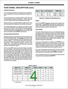
DATABUS BIT PERIOD
MINIMUM GAP GAP CLOCK
GAP DETECTION
TYPE
(ms)
(ms)
MHz
TIME (ms)
429
10
45
0.75
1.0
21.3 - 22.7
16 - 17
1.5
10.7 - 11.3
429
575
561
69 - 133
69 - 133
69 - 133
310 - 599
310 - 599
103 - 200
0.1
0.1
0.2
160 - 170
160 - 170
80 - 85
Table 1 - Typical Gap Detection Times
HOLT INTEGRATED CIRCUITS
3

 HOLTIC [ HOLT INTEGRATED CIRCUITS ]