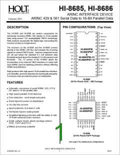
HI-8685, HI-8686
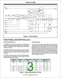
FUNCTIONAL DESCRIPTION (cont.)
ERROR CHECKING
Read
Byte
Data Bus Bits
ARINC Bits
Once a word gap is detected, the data word in the input reg-
ister is transferred to the receive buffer and checked for er-
rors.
1st
Byte 1
Byte 2
D0 - D15
D0 - D15
ARINC 1 - ARINC 16
ARINC 17 - ARINC 32
2nd
When parity detection is enabled (PARITY ENB high), the
received word is checked for odd parity. If there is a parity
error, the 32nd bit of the received data word is set high.
FIGURE 2. ORDER OF RECEIVED DATA
RESET
If parity checking is disabled (PARITY ENB low) the 32nd
bit of the data word is always the 32nd ARINC bit received.
A low on the RESET input sets a flip-flop which initializes the
internal logic. When RESET goes high, the internal logic re-
mains in the initialized state until the first word gap is de-
tected preventing reception of a partial word.
The ERROR flag output is set high upon receipt of a word
gap and the number of bits received since the previous
word gap is less than or greater than 32. The ERROR flag
is reset low when the next valid ARINC word is written into
the receive buffer or when RESET is pulsed low.
TEST MODE
The built-in differential line receiver can be disabled allowing
the data and clock detection circuitry to be driven directly
with digital signals. The logical OR function of the TESTA
and TESTB is defined in Truth Table 1. The two inputs can
be used for testing the receiver logic and for inputting ARINC
429 type data derived from another source/ protocol. See
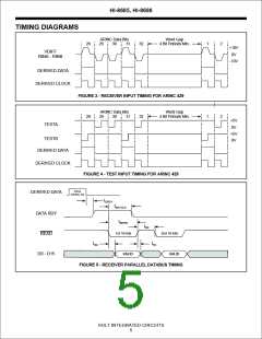
Figure 4 for typi cal test input timing.
READING RECEIVE BUFFER
When the data word is transferred to the receive buffer, the
DATA RDY pin goes high. The data word can then be read
in two 16-bit bytes by pulsing the READ input low as indi-
cated in Figure 5. The first read cycle resets DATA RDY
low and increments an internal counter to the second
16-bit byte. The relationship between each bit of an
ARINC word received and each bit of the two 16-bit data
bus bytes is specified in Figure 2.
The device should always be initialized with RESET imme-
diately after entering the test mode to clear a partial word
that may have been received since the last word gap. Oth-
erwise, an ERROR condition may occur and the first 32 bits
of data on the test inputs may not be properly received.
When a new ARINC word is received it always overwrites
the receive buffer. If the first byte of the previous word has
not been read, then previous data is lost and the receive
buffer will contain the new ARINC word. However, if the
DATA RDY pin goes high between the reading of the first
and second bytes, the first byte is no longer valid because
the corresponding second byte has been overwritten by
the new ARINC word. Also, the next read will be of the first
byte of the new ARINC word since the internal byte counter
is always reset to the first byte when new data is trans-
ferred to the receive buffer.
Also, when entering the test mode, both TESTA and TESTB
should be set high and held in that state for at least one
word gap period (17 gap clocks) after RESET goes high.
When exiting the test mode, both test inputs should be held
low and the device initialized with RESET.
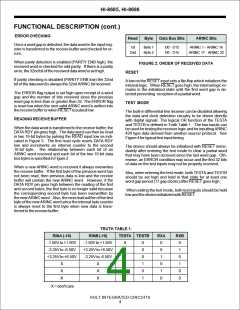
TRUTH TABLE 1.
RINB (-10) TESTA TESTB
RINA (-10)
RXA
RXB
-1.50V to +1.50V
-1.50V to +1.50V
0
0
0
0
1
1
0
0
0
1
0
1
0
0
1
0
1
0
0
1
0
1
0
0
-3.25V to -6.50V
+3.25V to +6.50V
+3.25V to +6.50V
-3.25V to -6.50V
X
X
X
X
X
X
X = don't care
HOLT INTEGRATED CIRCUITS
4

 HOLTIC [ HOLT INTEGRATED CIRCUITS ]