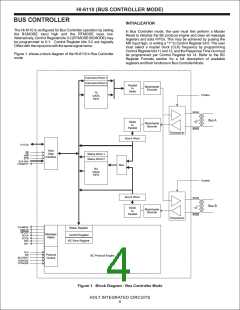
HI-6110 (BUS CONTROLLER MODE)
REGISTER FORMATS (BC Mode)
CONTROL REGISTER (R/W) Write Address: X1XX, Read Address: 1100
T
The Control Register settings determine HI-6110 operating
O
AR
Used
Used
mode, clock frequency and the bus enabled for transmit. It can
also be used to address registers for read/write operations, to
assert master reset, and to initiate MIL-STD-1553 message
sequences.
TMODE
TRB TRA R BCMOBDCESTMR
Not REPTNot CLKS
R
E
e
L
serRveAd3 RA2 RA1 RA0
X
X
0
X
0
1
MSB 15 14 13 12 11 10
9
8
7
6
5
4
3
2
1
0
LSB
BIT
15
NAME
-
FUNCTION
Not used in BC mode
Controls the time-out which causes the No Response Error.
14
REPTO
0
1
17 usec Gap (equivalent to 57 usec for 5.2.1.7 of the RTValidationTest Plan)
131 usec Gap
13
12
-
Not used in BC mode
CLKSEL
Selects the frequency of the HI-6110 external CLK input, as follows:
CLKSEL
Value
0
1
24 MHz
12 MHz
11
Reserved
RA3:0
This bit must be written to “0”.
10 - 7
Register Address for HI-6110 register and data read and write operations. The register address is defined by
the logical OR of these bits and their corresponding input pins. Writting Control Register bits 10:7 to 0000 is
necessary if the RA0 - RA3 input pins are used for HI-6110 register addressing.
6
-
Not used in BC mode
5 - 4
TRB, TRA
Setting either TRA or TRB to "1" enables transmit on MIL-STD-1553 BUS A or BUS B. Setting both TRA and
TRB selects neither bus. The BC protocol engine connects to the selected, active bus. The 1553 receiver,
Manchester decoder and RCV output signal are still operational on the inactive bus. Valid words received on the
inactive bus can be read without changing active bus by reading the Bus A Word or Bus B Word register.
NOTE: TheTXINHAandTXINHB input pins can override bus enablement.
3 - 2
RTMODE, HI-6110 mode select bits. These Control Register bits are logically OR'ed with their corresponding input pins,
BCMODE
allowing the user to select 1553 operating mode under either hardware or software control:
RTMODE BCMODE
1553 OPERATING MODE
0
0
1
1
0
1
0
1
Bus Monitor (MT), with assigned RTaddress
Bus Controller (BC)
RemoteTerminal (RT)
Bus Monitor (MT), without assigned RTaddress
1
0
BCSTART
MR
If initially reset, writing a "1" to this bit initiates a BC message sequence. This bit should be reset before next
message.
Master Reset. Writing "1" and then “0” to this bit performs the same function as pulsing the MR pin. All register
and data FIFOs are cleared when master reset is asserted. The Control Register is the exception; it is not
affected by Master Reset.
TRANSMIT DATA FIFO (Write only) Write Address: X010
The Transmit Data FIFO is 32-words deep and holds MIL-
STD-1553 message data. The FIFO is cleared on Master
Reset.
MIL-STD-1553 Message Data Word 15:0
15 14 13 12 11 10
9
8
7
6
5
4
3
2
1
0
Message data to be transmitted by the BC may be loaded into
the TRANSMIT DATA FIFO by the host prior to BCSTART.
Any data word must be loaded before mid-parity bit for the
1553 word it follows. Words are transmitted in the order they
are loaded.
MSB
LSB
RECEIVE DATA FIFO (Read only) Read Address: 0100
The Receive Data FIFO is 32-words deep and holds MIL-
STD-1553 message data. The FIFO is cleared by Master
Reset or when BCSTARToccurs.
MIL-STD-1553 Message Data Word 15:0
15 14 13 12 11 10
9
8
7
6
5
4
3
2
1
0
All MIL-STD-1553 data words received by the BC are stored in
the Receive DATA FIFO. A low FFEMPTY flag (output pin or
Status register bit) means message data is available to be
read by the host. Successive data reads cause FFEMPTY to
go high when the last word is read.
MSB
LSB
HOLT INTEGRATED CIRCUITS
5

 HOLTIC [ HOLT INTEGRATED CIRCUITS ]