HI-6110
PIN DESCRIPTIONS
SIGNAL
STR
FUNCTION
INPUT
INPUT
INPUT
I/O
DESCRIPTION
During I/O operations, data is latched on rising edge. (12K ohm pull-up resistor)
Device register access, READ = 1, WRITE = 0. (12K ohm pull-up resistor)
Chip Select for register reads and writes, active low. (12K ohm pull-down resistor)
Data bus signals. (12K ohm pull-down resistors)
R/W
CS
D0 - D15
RA0 - RA3
INPUTS
Register access address, inputs are ORed with corresponding Control register bits.
(12K ohm pull-down resistors)
BCSTART
INPUT
Message starts on rising edge when in BC mode. Input is ORed with a corresponding
Control register bit, where a 0 to 1 transition will also trigger message start. (This input
has a 12K ohm pull-down resistor.)
CLK
GND
MR
INPUT
POWER
INPUT
System Clock. (12K ohm pull-down resistor)
Power supply Ground, 0V.
Master Reset, active high. Clears all data FIFOs and all registers except the Control,
Transmit Status Word and Transmit Mode Data Word registers. This input is ORed
with a corresponding Control register bit. (12K ohm pull-down resistor)
ERROR goes high when a message error is detected.
ERROR
OUTPUT
In BC mode, ERROR resets when BCSTART is asserted to begin the next message.
For RT and MT modes, ERROR resets automatically after 3 to 4uS.
This output signal mirrors a corresponding Status register bit.
Goes high at the end of a valid message sequence. This output signal mirrors a
corresponding Status register bit.
VALMESS
FFEMPTY
RFLAG
OUTPUT
OUTPUT
OUTPUT
When low, data is available in the receive data FIFO for the active bus. This output
signal mirrors a corresponding Status register bit.
Flag for register writes of received message words other than Data words.
In BC mode: Goes low when a Status Word register is written.
In RT or MT mode: Goes low when either a Command word, Status word, or Mode
data word register is received and written in a register. This output mirrors a
corresponding Status register bit.
RF0 /
OUTPUT
OUTPUT
RF0 function: If a “1” when reading Bus A Word or Bus B Word registers, the stored
word had data sync.
RCVCMDA
RCVCMDA function: In RT mode or MT mode, RCVCMDA goes high when a valid
receive command has been decoded on Bus A.
This output mirrors a corresponding Status register bit.
RF1 /
RF1 function: If a “1” when reading Bus A Word or Bus B Word registers, the stored
word had command sync.
RCVCMDB
RCVCMDB function: In RT mode or MT mode, RCVCMDB goes high when a valid
receive command has been decoded on Bus B.
This output mirrors a corresponding Status register bit.
RCVA
RCVB
OUTPUTS Receive A and Receive B flags: In BC mode, these signals go high when any valid
word is received on Bus A or Bus B.
In RT or MT mode, these signals go high when a valid command is received on Bus A
or Bus B. For valid RT-to-RT only, RCV goes high after command word pair. These
output signals mirror two corresponding Status register bits.
TXINHA
TXINHB
INPUT
INPUT
XFMR
Logic one disables the Bus A transmitter. (12K ohm pull-up resistor)
Logic one disables the Bus B transmitter. (12K ohm pull-up resistor)
Positive and negative polarity of 1553 signals for Buses A and B. These signal pairs
connect the analog transceivers to the external transformer.
BUSA, BUSA
BUSB, BUSB
BCMODE
INPUT
INPUT
Selects operating mode. This input signal is ORed with a corresponding
Control register bit. (12K ohm pull-up resistor)
RTMODE
Selects operating mode. This input signal is ORed with a corresponding
Control register bit. (12K ohm pull-down resistor)
RTA0-RTA4
RTAP
INPUTS
INPUT
Remote Terminal address inputs, for RT mode. (12K ohm pull-up resistors)
This input sets Remote Terminal address parity, odd. (12K ohm pull-down resistor)
+3.3VDC 5% power supply input for internal logic
VDDLOG
POWER
VDDA, VDDB POWER
+3.3VDC 5% power supply inputs for Bus A and Bus B transceivers
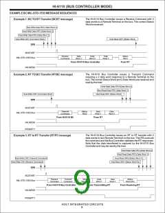
HOLT INTEGRATED CIRCUITS
2

 HOLTIC [ HOLT INTEGRATED CIRCUITS ]