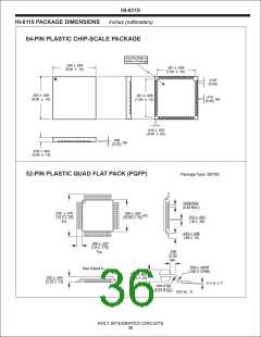
HI-6110
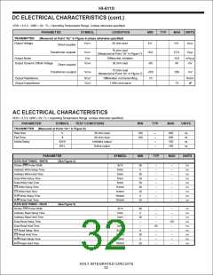
DC ELECTRICAL CHARACTERISTICS (cont.)
VDD = 3.3 V, GND = 0V, TA = Operating Temperature Range (unless otherwise specified)
PARAMETER
SYMBOL
CONDITION
MIN
TYP
MAX UNITS
TRANSMITTER
(Measured at Point “AD” in Figure 6 unless otherwise specified)
Output Voltage
VOUT
35 ohm load
6.0
9.0
Vp-p
Vp-p
Direct coupled
70 ohm load
(Measured at Point “AT“ in Figure 7)
Transformer coupled
VOUT
18.0
27.0
Output Noise
VON
Differential, inhibited
35 ohm load
10.0
90
mVp-p
mV
Output Dynamic Offset Voltage
VDYN
-90
Direct coupled
70 ohm load
(Measured at Point “AT“ in Figure 7)
Transformer coupled
VDYN
-250
10
250
15
mV
Output Resistance
Output Capacitance
ROUT
COUT
Differential, not transmitting
1 MHz sine wave
Kohm
pF
AC ELECTRICAL CHARACTERISTICS
VDD = 3.3 V, GND = 0V, TA = Operating Temperature Range (unless otherwise specified)
PARAMETER
SYMBOL
TEST CONDITIONS
MIN
TYP
MAX
UNITS
TRANSMITTER (Measured at Point “AD” in Figure 6)
Rise time
Fall Time
tr
35 ohm load
35 ohm load
100
100
--
--
--
--
300
300
100
150
ns
ns
ns
ns
tf
Inhibit Delay
tDI-H
tDI-L
Inhibited output
Active output
PARAMETER
(See Figure 4)
SYMBOL
MIN
TYP
MAX
UNITS
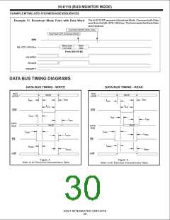
DATA BUS TIMING - WRITE
Strobe STR Pulse Width
Address Write Setup Time
Address Write Hold Time
Data Write Setup Time
Data Write Hold Time
CS Write Setup Time
tSTR
tAWS
50
0
--
--
--
--
--
--
--
--
--
--
--
--
--
--
--
--
--
--
ns
ns
ns
ns
ns
ns
ns
ns
ns
tAWH
30
30
30
50
30
0
tDWS
tDWH
tCSWS
tCSWH
tRWWS
tRWWH
CS Write Hold Time
R/W Write Setup Time
R/W Write Hold Time
30
DATA BUS TIMING - READ
Strobe STR Pulse Width
Address Read Setup Time
Address Read Hold Time
Data Read Setup Time
Data Read Hold Time
CS Read Setup Time
CS Read Hold Time
(See Figure 5)
tSTR
tARS
80
0
--
--
--
--
ns
ns
ns
ns
ns
ns
ns
ns
ns
tARH
30
--
--
--
tDRS
--
120
--
tDRH
--
60
--
tCSRS
tCSRH
tRWRS
tRWRH
0
--
30
0
--
--
R/W Read Setup Time
R/W Read Hold Time
--
--
30
--
--
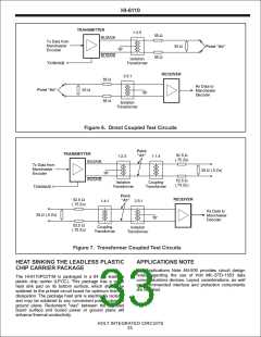
HOLT INTEGRATED CIRCUITS
32

 HOLTIC [ HOLT INTEGRATED CIRCUITS ]