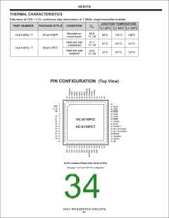
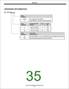
HI-6110
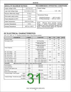
RECOMMENDED OPERATING CONDITIONS
ABSOLUTE MAXIMUM RATINGS
Supply Voltage
Supply voltage (VDD)
-0.3 V to +5 V
VDD....................................... 3.3V... 5%
Logic input voltage range
Receiver differential voltage
Driver peak output current
Power dissipation at 25°C
-0.3 V DC to +3.6 V
10 Vp-p
Temperature Range
+1.0 A
Industrial Screening.........-40°C to +85°C
Hi-Temp Screening........-55°C to +125°C
1.0 W
Solder Temperature
Junction Temperature
Storage Temperature
275°C for 10 sec.
175°C
NOTE:
Stresses above absolute maximum
ratings or outside recommended operating
conditions may cause permanent damage to the
device. These are stress ratings only. Operation
at the limits is not recommended.
-65°C to +150°C
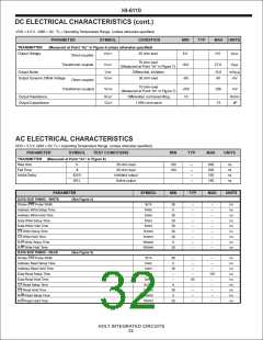
DC ELECTRICAL CHARACTERISTICS
VDD = 3.3 V, GND = 0V, TA = Operating Temperature Range (unless otherwise specified).
PARAMETER
SYMBOL
VDD
CONDITION
MIN
TYP
3.30
4
MAX
3.45
10
UNITS
V
Operating Voltage
3.15
Total Supply Current
ICC1
Not Transmitting
mA
Transmit one channel @
50% duty cycle
ICC2
225
425
250
mA
Transmit one channel @
100% duty cycle
ICC3
PD1
PD2
500
0.06
0.5
mA
W
Power Dissipation
Not Transmitting
Transmit one channel @
100% duty cycle
0.3
W
Min. Input Voltage
Max. Input Voltage
Min. Input Current
Max. Input Current
(HI)
(LO)
(HI)
VIH
VIL
IIH
Digital inputs
Digital inputs
70%
VDD
VDD
µA
30%
20
Digital inputs
(LO)
IIL
Digital inputs
-20
µA
Pull-Up / Pull-Down Current
Min. Output Voltage (HI)
Max. Output Voltage (LO)
IPUD
VOH
VIH
Digital inputs and data bus
IOUT = -1.0mA, Digital outputs
IOUT = 1.0mA, Digital outputs
275
µA
90%
VDD
VDD
10%
RECEIVER
(Measured at Point “AD“ in Figure 6 unless otherwise specified)
Input resistance
RIN
CIN
Differential
20
40
Kohm
pF
Input capacitance
Differential
5
Common mode rejection ratio
Input Level
CMRR
VIN
dB
Differential
9
Vp-p
V-pk
Vp-p
Vp-p
Vp-p
Vp-p
Input common mode voltage
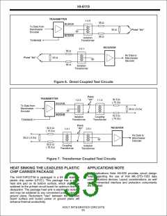
Threshold Voltage - Direct-coupled
VICM
VTHD
VTHND
VTHD
VTHND
-5.0
5.0
Detect
1.15
20.0
0.28
14.0
0.20
1 Mhz Sine Wave
(Measured at Point “AD“ in Figure 6)
No Detect
Theshold Voltage - Transformer-coupled Detect
0.86
1 MHz Sine Wave
(Measured at Point “AT“ in Figure 7)
No Detect
=
HOLT INTEGRATED CIRCUITS
31

 HOLTIC [ HOLT INTEGRATED CIRCUITS ]