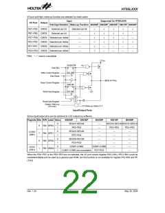
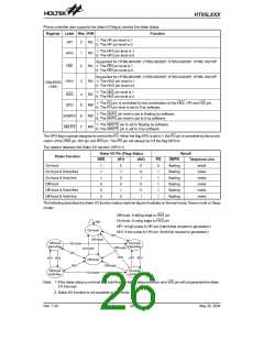
HT95LXXX
I/O port pull-high, wake-up function are selected by mask option
Input
Supported for HT95LXXX
I/O Port
Output
Pull-high Resistor Wake-up Function 400/40P 300/30P 200/20P 100/10P 000/00P
PA7~PA0 CMOS
PB7~PB0 CMOS
Selected per bit
Selected per bit
Selected per bit
Ö
Ö
Ö
Ö
Ö
Ö
Ö
Ö
Ö
Ö
Ö
Ö
Ö
*
¾
¾
¾
¾
¾
PD7~PD0 CMOS Selected per nibble
PE3~PE0 CMOS Selected per nibble
Ö
Ö
¾
Ö
¾
Ö
Ö
Ö
PF7~PF0
CMOS Selected per nibble
¾
¾
¾
¾
¾
¾
¾
¾
PG3~PG0 CMOS Selected per nibble
Note:
²¾² means unavailable
V
D
D
C
o
n
t
r
o
l
B
i
t
P
U
D
a
t
a
B
u
s
D
C
Q
K
Q
B
W
r
i
t
e
C
o
n
t
r
o
l
R
e
g
i
s
t
e
r
S
C
h
i
p
R
e
s
e
t
A
l
l
I
/
O
P
i
n
s
R
e
a
d
C
o
n
t
r
o
l
R
e
g
i
s
t
e
r
D
a
t
a
B
i
t
D
C
Q
K
Q
B
W
r
i
t
e
D
a
t
a
R
e
g
i
s
t
e
r
S
M
U
X
R
e
a
d
D
a
t
a
R
e
g
i
s
t
e
r
S
y
s
t
e
m
W
a
k
e
-
u
p
P
A
W
a
k
e
-
u
p
O
p
t
i
o
n
0
~
7
(
P
A
o
n
l
y
)
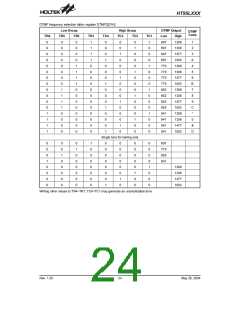
Input/Output Ports
Some input/output pins can be optioned to LCD outputs by software.
Register Bits R/W Label Value
400/40P
300/30P
200/20P
100/10P
000/00P
0
SEG47~SEG44
SEG19~SEG16 SEG15~SEG12
¾
¾
¾
¾
¾
¾
5
7
6
1
RW SPE0
RW SPD1
RW SPD0
RW VBIAS
1
0
1
0
1
0
1
PE3~PE0
SEG43~SEG40
PD7~PD4
PE3~PE0
PE3~PE0
¾
¾
¾
¾
¾
¾
¾
¾
¾
¾
¾
¾
LCDIO
(28H)
SEG39~SEG36
PD3~PD0
COM7~COM0
COM7~COM0
PD7~PD0
LCDC
(2DH)
COM7~COM0 are unavailable
When the PD0~PD7 or the PE0~PE3 are not selected, the I/O port control register PDC(19H), PEC(1BH) could be
readable/writable and be used as a general user RAM, but this function is not available for register PD(18H) and PE
(1AH).
Rev. 1.20
22
May 26, 2004

 HOLTEK [ HOLTEK SEMICONDUCTOR INC ]