HT48R063/064/065/066/0662/067
f
S
Y
S
[
[
[
[
P
P
P
P
W
W
W
W
M
M
M
M
]
]
]
]
=
=
=
=
1
1
1
1
0
0
0
0
0
1
2
3
P
P
P
P
W
W
W
W
M
M
M
M
2
5
/
6
4
2
2
2
2
5
5
6
6
/
/
/
/
6
6
6
6
4
4
4
4
2
2
2
2
5
5
5
6
/
/
/
/
6
6
6
6
4
4
4
4
2
5
/
6
4
2
2
2
2
5
6
6
6
/
/
/
/
6
6
6
6
4
4
4
4
2
2
2
6
6
6
/
/
/
6
6
6
4
4
4
2
2
2
5
5
5
/
/
/
6
6
6
4
4
4
P
W
M
m
o
d
u
l
a
S
t
Y
i
S
o
n
p
e
r
i
o
d
:
6
4
/
f
M
o
d
u
l
a
t
i
o
n
M
c
o
y
d
c
u
l
l
e
a
t
0
i
o
n
M
c
o
y
d
c
u
l
l
e
a
t
1
i
o
n
M
c
o
y
d
c
u
l
l
e
a
t
2
i
o
n
M
c
o
y
d
c
u
l
l
e
a
t
3
i
o
P
W
M
c
y
S
c
Y
l
S
e
:
2
5
6
/
f
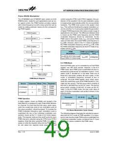
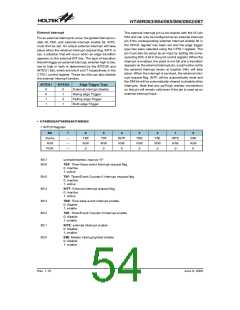
6+2 PWM Mode
b
7
b
0
P
W
M
R
e
g
i
s
t
e
r
(
6
A
D
C
v
a
l
u
u
e
C
v
a
l
e
PWM Register for 6+2 Mode
7+1 PWM Mode
PWM Output Control
Each full PWM cycle, as it is controlled by an 8-bit PWM
register, has 256 clock periods. However, in the 7+1
PWM mode, each PWM cycle is subdivided into two indi-
vidual sub-cycles known as modulation cycle 0 ~ modula-
tion cycle 1, denoted as i in the table. Each one of these
two sub-cycles contains 128 clock cycles. In this mode, a
modulation frequency increase of two is achieved. The
8-bit PWM register value, which represents the overall
duty cycle of the PWM waveform, is divided into two
groups. The first group which consists of bit1~bit7 is de-
noted here as the DC value. The second group which
consists of bit0 is known as the AC value. In the 7+1
PWM mode, the duty cycle value of each of the two mod-
ulation sub-cycles is shown in the following table.
The PWM outputs are pin-shared with the I/O pins PA4,
PC2 and PC3. To operate as a PWM output and not as
an I/O pin, the correct bits must be set in the CTRL0 and
CTRL2 register. A zero value must also be written to the
corresponding bit in the I/O port control register PAC.4,
PCC.2 and PCC.3 to ensure that the corresponding
PWM output pin is setup as an output. After these two
initial steps have been carried out, and of course after
the required PWM value has been written into the
PWMn register, writing a high value to the correspond-
ing bit in the output data register PA.4, PC.2 and PC.3
will enable the PWM data to appear on the pin. Writing a
zero value will disable the PWM output function and
force the output low. In this way, the Port data output
registers can be used as an on/off control for the PWM
function. Note that if the CTRL0 and CTRL2 registers
have selected the PWM function, but a high value has
been written to its corresponding bit in the PAC or PCC
control register to configure the pin as an input, then the
pin can still function as a normal input line, with pull-high
resistor options.
DC
Parameter
AC (0~1)
i<AC
(Duty Cycle)
DC+1
128
Modulation cycle i
(i=0~1)
DC
i³AC
128
7+1 Mode Modulation Cycle Values
The following diagram illustrates the waveforms associ-
ated with the 7+1 mode PWM operation. It is important
to note how the single PWM cycle is subdivided into 2 in-
dividual modulation cycles, numbered 0 and 1 and how
the AC value is related to the PWM value.
Rev. 1.10
50
June 9, 2009

 HOLTEK [ HOLTEK SEMICONDUCTOR INC ]