HT46R01B/02B/01N/02N
HT48R01B/02B/01N/02N
·
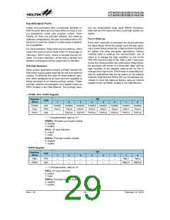
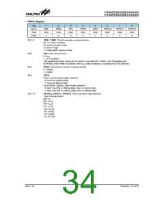
I/O Port Control Registers
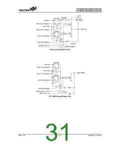
PFD Output
The PFD function output is pin-shared with an I/O pin.
The output function of this pin is chosen using the
CTRL0 register. Note that the corresponding bit of the
port control register, must setup the pin as an output
to enable the PFD output. If the port control register
has setup the pin as an input, then the pin will function
as a normal logic input with the usual pull-high selec-
tion, even if the PFD function has been selected.
Each Port has its own control register, known as PAC,
PBC, which controls the input/output configuration. With
this control register, each I/O pin with or without
pull-high resistors can be reconfigured dynamically un-
der software control. For the I/O pin to function as an in-
put, the corresponding bit of the control register must be
written as a ²1². This will then allow the logic state of the
input pin to be directly read by instructions. When the
corresponding bit of the control register is written as a
²0², the I/O pin will be setup as a CMOS output. If the pin
is currently setup as an output, instructions can still be
used to read the output register. However, it should be
noted that the program will in fact only read the status of
the output data latch and not the actual logic status of
the output pin.
·
PWM Outputs
The PWM function whose outputs are pin-shared with
I/O pins. The PWM output functions are chosen using
the CTRL0 register. Note that the corresponding bit of
the port control registers, for the output pin, must
setup the pin as an output to enable the PWM output.
If the pins are setup as inputs, then the pin will function
as a normal logic input with the usual pull-high selec-
tions, even if the PWM registers have enabled the
PWM function.
Pin-shared Functions
·
A/D Inputs
The flexibility of the microcontroller range is greatly en-
hanced by the use of pins that have more than one func-
tion. Limited numbers of pins can force serious design
constraints on designers but by supplying pins with
multi-functions, many of these difficulties can be over-
come. For some pins, the chosen function of the
multi-function I/O pins is set by configuration options
while for others the function is set by application pro-
gram control.
Each device in this series has either four or eight in-
puts to the A/D converter. All of these analog inputs
are pin-shared with I/O pins on Port B. If these pins
are to be used as A/D inputs and not as I/O pins then
the corresponding PCRn bits in the A/D converter
control register, ADCR, must be properly setup. There
are no configuration options associated with the A/D
converter. If chosen as I/O pins, then full pull-high re-
sistor configuration options remain, however if used
as A/D inputs then any pull-high resistor options asso-
ciated with these pins will be automatically discon-
nected.
·
External Interrupt Input
The external interrupt pin, INT, is pin-shared with an
I/O pin. To use the pin as an external interrupt input
the correct bits in the INTC0 register must be pro-
grammed. The pin must also be setup as an input by
setting the PAC3 bit in the Port Control Register. A
pull-high resistor can also be selected via the appro-
priate port pull-high resistor register. Note that even if
the pin is setup as an external interrupt input the I/O
function still remains.
·
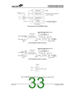
External Timer/Event Counter Input
The Timer/Event Counter pins, TC0 and TC1 are
pin-shared with I/O pins. For these shared pins to be
used as Timer/Event Counter inputs, the Timer/Event
Counter must be configured to be in the Event Coun-
ter or Pulse Width Capture Mode. This is achieved by
setting the appropriate bits in the Timer/Event Counter
Control Register. The pins must also be setup as in-
puts by setting the appropriate bit in the Port Control
Register. Pull-high resistor options can also be se-
lected using the port pull-high resistor registers. Note
that even if the pin is setup as an external timer input
the I/O function still remains.
Rev.1.10
30
February 12, 2010

 HOLTEK [ HOLTEK SEMICONDUCTOR INC ]