HT46R01B/02B/01N/02N
HT48R01B/02B/01N/02N
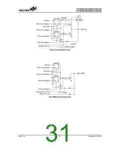
Input/Output Ports
Holtek microcontrollers offer considerable flexibility on
their I/O ports. Most pins can have either an input or out-
put designation under user program control. Addi-
tionally, as there are pull-high resistors and wake-up
software configurations, the user is provided with an I/O
structure to meet the needs of a wide range of applica-
tion possibilities.
tors are implemented using weak PMOS transistors.
Note that pin PA7 does not have a pull-high resistor se-
lection.
Port A Wake-up
If the HALT instruction is executed, the device will enter
the Sleep Mode, where the system clock will stop result-
ing in power being conserved, a feature that is important
for battery and other low-power applications. Various
methods exist to wake-up the microcontroller, one of
which is to change the logic condition on one of the
PA0~PA7 pins from high to low. After a HALT instruction
forces the microcontroller into entering the Sleep Mode,
the processor will remain in a low-power state until the
logic condition of the selected wake-up pin on Port A
changes from high to low. This function is especially suit-
able for applications that can be woken up via external
switches. Note that pins PA0 to PA7 can be selected indi-
vidually to have this wake-up feature using an internal
register known as PAWK, located in the Data Memory.
For input operation, these ports are non-latching, which
means the inputs must be ready at the T2 rising edge of
instruction ²MOV A,[m]², where m denotes the port ad-
dress. For output operation, all the data is latched and
remains unchanged until the output latch is rewritten.
Pull-high Resistors
Many product applications require pull-high resistors for
their switch inputs usually requiring the use of an external
resistor. To eliminate the need for these external resis-
tors, when configured as an input have the capability of
being connected to an internal pull-high resistor. These
pull-high resistors are selectable via a register known as
PAPU located in the Data Memory. The pull-high resis-
·
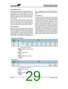
PAWK, PAC, PAPU Register
Bit
Register
POR
Name
7
6
5
4
3
2
1
0
PAWK
PAC
00H
FFH
00H
PAWK7 PAWK6 PAWK5 PAWK4 PAWK3 PAWK2 PAWK1 PAWK0
PAC7
PAC6
PAC5
PAC4
PAC3
PAC2
PAC1
PAC0
PAPU
PAPU6
PAPU5
PAPU4
PAPU3
PAPU2
PAPU1
PAPU0
¾
²¾² Unimplemented, read as ²0²
PAWKn: PA wake-up function enable
0: disable
1: enable
PACn: I/O type selection
0: output
1: input
PAPUn: Pull-high function enable
0: disable
1: enable
·
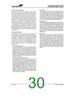
PBPU Register
Register
Bit
POR
Name
7
6
5
4
3
2
1
0
PBC
FFH
00H
PBC1
PBPU1
PBC0
PBPU0
¾
¾
¾
¾
¾
¾
¾
¾
¾
¾
¾
¾
PBPU
²¾² Unimplemented, read as ²0²
PBCn: I/O type selection
0: output
1: input
PBPUn: Pull-high function enable
0: disable
1: enable
Rev.1.10
29
February 12, 2010

 HOLTEK [ HOLTEK SEMICONDUCTOR INC ]