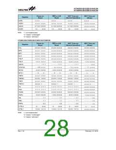
HT46R01B/02B/01N/02N
HT48R01B/02B/01N/02N
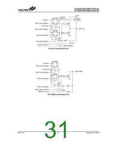
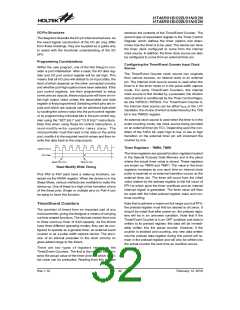
I/O Pin Structures
retrieves the contents of the Timer/Event Counter. The
second type of associated register is the Timer Control
Register which defines the timer options and deter-
mines how the timer is to be used. The device can have
the timer clock configured to come from the internal
clock source. In addition, the timer clock source can also
be configured to come from an external timer pin.
The diagrams illustrate the I/O pin internal structures. As
the exact logical construction of the I/O pin may differ
from these drawings, they are supplied as a guide only
to assist with the functional understanding of the I/O
pins.
Programming Considerations
Configuring the Timer/Event Counter Input Clock
Source
Within the user program, one of the first things to con-
sider is port initialisation. After a reset, the I/O data reg-
ister and I/O port control register will be set high. This
means that all I/O pins will default to an input state, the
level of which depends on the other connected circuitry
and whether pull-high options have been selected. If the
port control registers, are then programmed to setup
some pins as outputs, these output pins will have an ini-
tial high output value unless the associated port data
register is first programmed. Selecting which pins are in-
puts and which are outputs can be achieved byte-wide
by loading the correct value into the port control register
or by programming individual bits in the port control reg-
ister using the ²SET [m].i² and ²CLR [m].i² instructions.
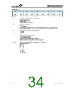
Note that when using these bit control instructions, a
read-modify-write operation takes place. The
microcontroller must first read in the data on the entire
port, modify it to the required new bit values and then re-
write this data back to the output ports.
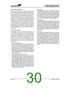
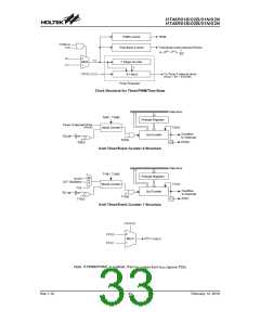
The Timer/Event Counter clock source can originate
from various sources, an internal clock or an external
pin. The internal clock source source is used when the
timer is in the timer mode or in the pulse width capture
mode. For some Timer/Event Counters, this internal
clock source is first divided by a prescaler, the division
ratio of which is conditioned by the Timer Control Regis-
ter bits T0PSC0~T0PSC2. For Timer/Event Counter 0,
the internal clock source can be either fSYS or the LXT
Oscillator, the choice of which is determined by the T0S
bit in the TMR0C register.
An external clock source is used when the timer is in the
event counting mode, the clock source being provided
on an external timer pin TCn. Depending upon the con-
dition of the TnEG bit, each high to low, or low to high
transition on the external timer pin will increment the
counter by one.
T
1
T
2
T
3
T
4
T
1
T
2
T
3
T
4
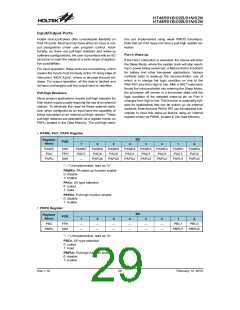
Timer Registers - TMR0, TMR1
S
y
s
t
e
m
C
l
o
c
k
The timer registers are special function registers located
in the Special Purpose Data Memory and is the place
where the actual timer value is stored. These registers
are known as TMR0 and TMR1. The value in the timer
registers increases by one each time an internal clock
pulse is received or an external transition occurs on the
external timer pin. The timer will count from the initial
value loaded by the preload register to the full count of
FFH at which point the timer overflows and an internal
interrupt signal is generated. The timer value will then
be reset with the initial preload register value and con-
tinue counting.
P
o
r
t
D
a
t
a
R
e
a
d
f
r
o
m
P
W
o
r
r
i
t
t
e
t
o
P
o
r
t
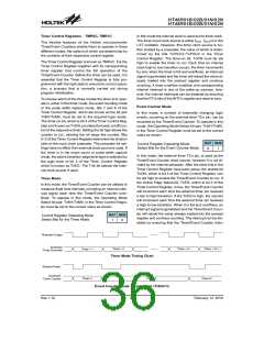
Read Modify Write Timing
Pins PA0 to PA7 each have a wake-up functions, se-
lected via the PAWK register. When the device is in the
Sleep Mode, various methods are available to wake the
device up. One of these is a high to low transition of any
of the these pins. Single or multiple pins on Port A can
be setup to have this function.
Note that to achieve a maximum full range count of FFH,
the preload register must first be cleared to all zeros. It
should be noted that after power-on, the preload regis-
ters will be in an unknown condition. Note that if the
Timer/Event Counter is in an OFF condition and data is
written to its preload register, this data will be immedi-
ately written into the actual counter. However, if the
counter is enabled and counting, any new data written
into the preload data register during this period will re-
main in the preload register and will only be written into
the actual counter the next time an overflow occurs.
Timer/Event Counters
The provision of timers form an important part of any
microcontroller, giving the designer a means of carrying
out time related functions. The devices contain from one
to three count-up timer of 8-bit capacity. As the timers
have three different operating modes, they can be con-
figured to operate as a general timer, an external event
counter or as a pulse width capture device. The provi-
sion of an internal prescaler to the clock circuitry on
gives added range to the timers.
There are two types of registers related to the
Timer/Event Counters. The first is the register that con-
tains the actual value of the timer and into which an ini-
tial value can be preloaded. Reading from this register
Rev.1.10
32
February 12, 2010

 HOLTEK [ HOLTEK SEMICONDUCTOR INC ]