HT46R01B/02B/01N/02N
HT48R01B/02B/01N/02N
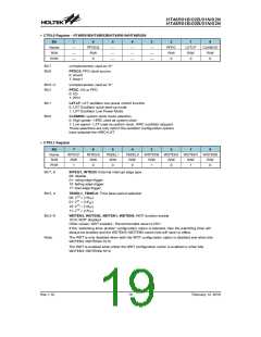
Input/Output Ports and Control Registers
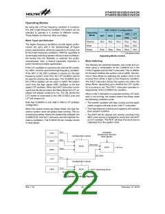
System Control Registers - CTRL0, CTRL1
Within the area of Special Function Registers, the port
PA, PB, etc data I/O registers and their associated con-
trol register PAC, PBC, etc play a prominent role. These
registers are mapped to specific addresses within the
Data Memory as shown in the Data Memory table. The
data I/O registers, are used to transfer the appropriate
output or input data on the port. The control registers
specifies which pins of the port are set as inputs and
which are set as outputs. To setup a pin as an input, the
corresponding bit of the control register must be set
high, for an output it must be set low. During program in-
itialisation, it is important to first setup the control regis-
ters to specify which pins are outputs and which are
inputs before reading data from or writing data to the I/O
ports. One flexible feature of these registers is the ability
to directly program single bits using the ²SET [m].i² and
²CLR [m].i² instructions. The ability to change I/O pins
from output to input and vice versa by manipulating spe-
cific bits of the I/O control registers during normal pro-
gram operation is a useful feature of these devices.
These registers are used to provide control over various
internal functions. Some of these include the PFD con-
trol, PWM control, certain system clock options, the LXT
Oscillator low power control, external Interrupt edge trig-
ger type, Watchdog Timer enable function, Time Base
function division ratio, and the LXT oscillator enable
control.
Wake-up Function Register - PAWK
When the microcontroller enters the Sleep Mode, vari-
ous methods exist to wake the device up and continue
with normal operation. One method is to allow a falling
edge on the I/O pins to have a wake-up function. This
register is used to select which Port A I/O pins are used
to have this wake-up function.
Pull-high Registers - PAPU, PBPU
The I/O pins, if configured as inputs, can have internal
pull-high resistors connected, which eliminates the need
for external pull-high resistors. This register selects which
I/O pins are connected to internal pull-high resistors.
·
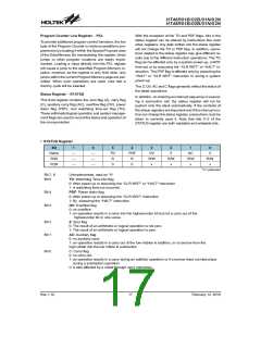
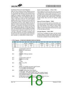
CTRL0 Register - HT46R01B/HT46R02B/HT46R01N/HT46R02N
Bit
Name
R/W
7
6
PFDCS
R/W
0
5
PWMSEL
R/W
4
3
PWMC0
R/W
0
2
PFDC
R/W
0
1
LXTLP
R/W
0
0
CLKMOD
R/W
¾
¾
¾
¾
¾
¾
POR
0
0
Bit 7
unimplemented, read as ²0²
Bit 6
Bit 5
PFDCS: PFD clock source
0: timer0
1: timer1
PWMSEL: PWM type selection
0: 6+2
1: 7+1
Bit 4
Bit 3
unimplemented, read as ²0²
PWMC0: I/O or PWM
0: I/O
1: PWM
Bit 2
Bit 1
Bit 0
PFDC: I/O or PFD
0: I/O
1: PFD
LXTLP: LXT oscillator low power control function
0: LXT Oscillator quick start-up mode
1: LXT Oscillator Low Power Mode
CLKMOD: system clock mode selection.
0: High speed - HIRC used as system clock
1: Low speed - LXT used as system clock, HIRC oscillator stopped.
These selections are only valid if the oscillator configuration options
have selected the HIRC+LXT.
Note:
If PWM output is selected by PWMC0 bit, fTP comes always from fSYS
.
(fTP is the clock source for timer0/2, time base and PWM)
Rev.1.10
18
February 12, 2010

 HOLTEK [ HOLTEK SEMICONDUCTOR INC ]