Preliminary
HT48R06A-1
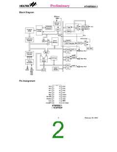
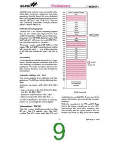
Pin Description
ROM Code
Option
Pin No. Pin Name I/O
Description
Bidirectional 8-bit input/output port. Each bit can be
configured as wake-up input by ROM code option.
Software instructions determine the CMOS output or
schmitt trigger input with a pull-high resistor (deter-
mined by pull-high options).
4~1
18~15
Pull-high*
Wake-up
PA0~PA7
I/O
Bidirectional 3-bit input/output port. Software in-
structions determine the CMOS output or schmitt
trigger input with a pull-high resistor (determined by
7
6
5
PB0/BZ
PB1/BZ
PB2
Pull-high* pull-high options).
I/O or
BZ/BZ
I/O
The PB0 and PB1 are pin-shared with the BZ and BZ,
respectively. Once the PB0 and PB1 are selected as
buzzer driving outputs, the output signals come from
an internal PFD generator (shared with timer/event
counter).
8
VSS
Negative power supply, ground
¾
¾
Bidirectional I/O lines. Software instructions deter-
mine the CMOS output or SCHMITT trigger input
with a pull-high resistor (determined by pull-high op-
9
10
PC0/INT
PC1/TMR
I/O Pull-high* tions). The external interrupt and timer input are
pin-shared with the PC0 and PC1, respectively. The
external interrupt input is activated on a high to low
transition.
11
12
RES
VDD
I
Schmitt trigger reset input. Active low
Positive power supply
¾
¾
¾
OSC1, OSC2 are connected to an RC network or Crys-
tal (determined by ROM code option) for the internal
system clock. In the case of RC operation, OSC2 is the
output terminal for 1/4 system clock.
13
14
OSC1
OSC2
I
Crystal
or RC
O
* All pull-high resistors are controlled by an option bit.
Absolute Maximum Ratings
Supply Voltage ...............VSS-0.3V to VSS+5.5V
Input Voltage.................VSS-0.3V to VDD+0.3V
Storage Temperature.................-50°C to 125°C
Operating Temperature ..............-40°C to 85°C
Note: These are stress ratings only. Stresses exceeding the range specified under "Absolute Maxi-
mum Ratings" may cause substantial damage to the device. Functional operation of this device
at other conditions beyond those listed in the specification is not implied and prolonged expo-
sure to extreme conditions may affect device reliability.
3
February 25, 2000

 HOLTEK [ HOLTEK SEMICONDUCTOR INC ]