Preliminary
HT48R06A-1
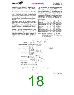
The related pins of OTP programming and veri-
fication are listed in the following table.
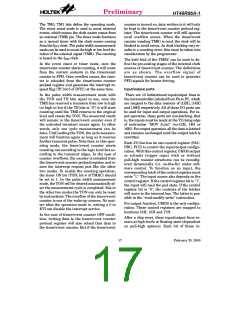
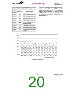
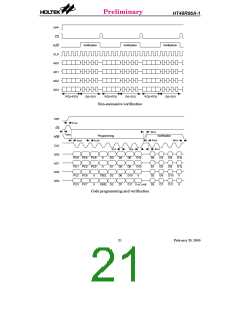
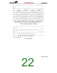
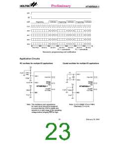
The timing charts of programming and verifica-
tion are as shown. There is a LOCK signal for
code protection. If the LOCK is "1", reading the
code will return the result "1". However, if the
LOCK is "0", the code protection is disabled and
the code can be read always until the LOCK is
programmed as "1".
Pin
Name
Function
Description
PA0
AD0
AD1
AD2
AD3
Bit 0 of address/data bus
Bit 1 of address/data bus
Bit 2 of address/data bus
Bit 3 of address/data bus
PA1
PA2
PA3
Serial clock input for ad-
dress and data
PA4
CLK
PA5
PA6
CS
Chip select, active low
Read/write control input
R/W
Programming the power
supply
RES
VPP
V
P
P
C
S
R
C
A
A
A
A
/
L
W
K
V
e
r
i
f
i
c
a
t
i
o
n
V
e
r
i
f
i
c
a
t
i
o
n
D
D
D
D
0
1
2
3
P
P
P
P
C
C
C
C
0
1
2
3
P
C
4
0
0
P
C
D
D
D
D
8
0
1
2
3
D
D
D
4
5
6
D
8
D
D
1
1
2
3
D
D
D
D
0
1
2
3
D
D
D
D
4
5
6
7
D
D
D
D
8
9
1
1
D
D
D
D
0
1
2
3
D
D
1
1
2
3
P
P
C
C
5
6
P
C
9
D
D
D
9
1
1
0
0
T
S
E
L
0
1
0
0
1
0
0
P
C
7
O
S
E
L
D
7
0
P
C
i
n
c
r
e
s
i
n
g
a
u
t
o
m
a
t
i
c
a
l
l
y
Successive verification
20
February 25, 2000

 HOLTEK [ HOLTEK SEMICONDUCTOR INC ]