Preliminary
HT48R06A-1
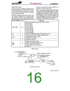
The PC0 and PC1 are pin-shared with INT,
TMR and pins respectively.
edge of PA4 (CLK) for OTP programming and
verification.
It is recommended that unused or not bonded
out I/O lines should be set as output pins by
software instruction to avoid consuming power
under input floating state.
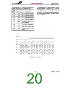
The address data contains the code address (11
bits) and two option bits. A complete write cycle
will contain four CLK cycles. The first cycle,
bits 0~3 of the address are latched into the
device. The second and third cycles, bits 4~7
and bits 8~9 are latched respectively. The
fourth cycle, bit 2 is the TSEL option bit and bit
3 is the OSEL option bit. Bits 2~3 in the third
cycle and bits 0~1 in the fourth cycle are unde-
fined. If the TSEL is "1" and the OSEL is "0",
the TEST memory will be read. If the TSEL is
"0" and the OSEL is "1", the option memory will
be accessed. If both the TSEL and OSEL are
"0", the program memory will be managed.
ROM code option
The following table shows all kinds of ROM
code option in the microcontroller. All of the
ROM code options must be defined to ensure
proper system functioning.
Items
Option
1
2
3
WDT clock source: WDTOSC/fTID
WDT enable/disable: enable/disable
LVD enable/disable: enable/disable
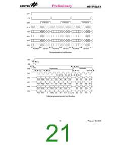
The code data is 14 bits wide. A complete
read/write cycle contains four CLK cycles. In
the first cycle, bits 0~3 of the code data are ac-
cessed. In the second and third, bits 4~7 and
bits 8~11 are accessed respectively. In the
fourth cycle, bits 12~13 are accessed. Bits
14~15 are undefined. During code verification,
reading will return the result "00".
CLRWDT instruction(s)
: one/two clear WDT
instruction(s)
4
5
6
System oscillator: RC/Crystal
Pull-high resistors (PA~PC):
none/pull-high
Select the TSEL and OSEL to program and
verify the program memory and option
memory. Use the R/W (PA6) to select between
programming or verification.
7
8
9
BZ option: disable/enable
PA0~PA7 wake-up: disable/enable
Lock: unlock/lock
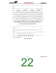
The address is incremented by one automati-
cally after a code verification cycle. If the dis-
continued address programming or
verification is accomplished, the automatic ad-
dressing increment is disabled. For the discon-
tinued address programming and verification,
the CS pin must return to high level for a pro-
gramming or verification cycle, that is, if a dis-
continued address is managed, the
programming or verification cycle must be in-
terrupted and restarted as well.
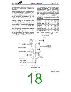
PROM programming and verification
The program memory used in the
microcontroller is arranged into a 1024´14 bits
program memory and a 3´8 bits option memory.
The program code and option code are stored in
the program and option memories. The pro-
gramming of memories can be summarized in
nine steps as described below:
·
·
·
Power on (VDD=6.25V)
Set VPP (RES) to 12.5V
Set CS (PA5) to low
Let PA3~PA0 (AD3~AD0) be the address and
data bus and the PA4 (CLK) be the clock input.
The data on the AD3~AD0 pins will be clocked
into or out of the microcontroller on the falling
19
February 25, 2000

 HOLTEK [ HOLTEK SEMICONDUCTOR INC ]