HT46R064G/065G/0662G
Enhanced A/D Type 8-Bit OTP MCU with OPA
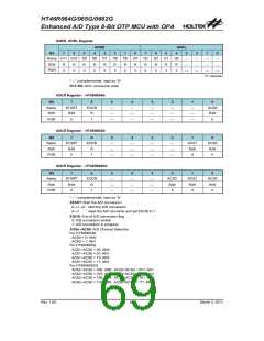
PCR Register - HT46R064G
Bit
Name
R/W
7
6
5
4
3
2
1
PCR1
R/W
0
0
PCR0
R/W
0
¾
¾
¾
¾
¾
¾
¾
¾
¾
¾
¾
¾
¾
¾
¾
¾
¾
¾
POR
PCR Register - HT46R065G
Bit
Name
R/W
7
6
5
4
3
PCR3
R/W
0
2
PCR2
R/W
0
1
PCR1
R/W
0
0
PCR0
R/W
0
¾
¾
¾
¾
¾
¾
¾
¾
¾
¾
¾
¾
POR
²¾² unimplemented, read as ²0²
PCRn: define the analog input configuration (A/D input or not)
0: I/O or other pin-shared function
1: A/D input (ANn input)
Note: If all the PCRn bits are zero, all the A/D analog input channels will be disabled and the A/D
converter circuitry will be powered off.
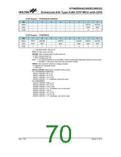
ANCSR Register - HT46R0662G
Bit
Name
R/W
7
PCR7
R/W
0
6
PCR6
R/W
0
5
PCR5
R/W
0
4
PCR4
R/W
0
3
PCR3
R/W
0
2
PCR2
R/W
0
1
PCR1
R/W
0
0
PCR0
R/W
0
POR
PCRn: define the analog input configuration (A/D input or not)
0: I/O or other pin-shared function
1: A/D input (ANn input)
A/D Operation
The START bit in the register is used to start and reset the A/D converter. When the microcontroller
sets this bit from low to high and then low again, an analog to digital conversion cycle will be initi-
ated. When the START bit is brought from low to high but not low again, the EOCB bit in the ADCR
register will be set to 1 and the analog to digital converter will be reset. It is the START bit that is
used to control the overall start operation of the internal analog to digital converter.
The EOCB bit in the ADCR register is used to indicate when the analog to digital conversion process
is complete. This bit will be automatically set to 0 by the microcontroller after a conversion cycle has
ended. In addition, the corresponding A/D interrupt request flag will be set in the interrupt control
register, and if the A/D interrupt is enabled, an appropriate internal interrupt signal will be gener-
ated. This A/D internal interrupt signal will direct the program flow to the associated A/D internal in-
terrupt address for processing. If the A/D internal interrupt is disabled, the microcontroller can be
used to poll the EOCB bit in the ADCR register to check whether it has been cleared as an alternative
method of detecting the end of an A/D conversion cycle.
The clock source for the A/D converter, which originates from the system clock fSYS, is first divided by
a division ratio, the value of which is determined by the ADCS2, ADCS1 and ADCS0 bits in the
ACSR register.
Rev. 1.00
71
March 3, 2011

 HOLTEK [ HOLTEK SEMICONDUCTOR INC ]