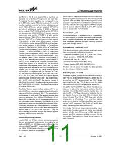
HT46RU66/HT46CU66
The function of data movement between two indirect ad-
dressing registers is not supported. The memory pointer
registers, MP0 and MP1, are both 8-bit registers used to
access the Data Memory in combination with their corre-
sponding indirect addressing registers. MP0 can only be
used to access data from Bank 0, while MP1 can be
used to access data from all banks.
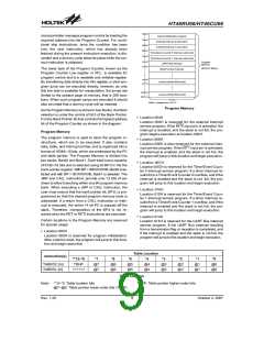
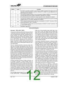
and Bank 3: 192´8 bits). Most of these registers are
readable and writeable, although some are read only.
The special function registers are overlapped in any
bank. Of the two types of functional groups, the special
function registers consist of an Indirect addressing reg-
ister 0 (00H), a Memory pointer register 0 (MP0;01H),
an Indirect addressing register 1 (02H), a Memory
pointer register 1 (MP1;03H), a Bank pointer (BP;04H),
an Accumulator (ACC;05H), a Program counter
lower-order byte register (PCL;06H), a table pointer
lower-order byte (TBLP;07H), a table pointer higher-or-
der byte (TBHP;1FH), a Table higher-order byte register
(TBLH;08H), a Real time clock control register
(RTCC;09H), a Status register (STATUS;0AH), an Inter-
rupt control register 0 (INTC0;0BH), a Timer/Event
Counter 0 (TMR0H;0CH; TMR0L;0DH), a Timer/Event
Counter 0 control register (TMR0C;0EH), a Timer/Event
Counter 1 (TMR1H:0FH;TMR1L;10H), a Timer/Event
Counter 1 control register (TMR1C;11H), a Timer/Event
Counter 2 (TMR2;2DH), a Timer/Event Counter 2 con-
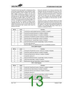
trol register (TMR2C;2EH), Interrupt control register 1
(INTC1;1EH), Multi-function Interrupt control register 1
(MFIC;2FH), PWM data register (PWM0;1AH,
PWM1;1BH, PWM2;1CH, PWM3;1DH), the A/D result
lower-order byte register (ADRL;24H), the A/D result
higher-order byte register (ADRH;25H), the A/D control
register (ADCR;26H), the A/D clock setting register
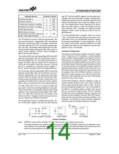
(ACSR;27H), I/O registers (PA;12H, PB;14H, PC;16H,
PD;18H) and I/O control registers (PAC;13H, PBC;15H,
PCC;17H, PDC;19H), the UART Bus status register
control register (USR;30H), the UART Bus control regis-
ter 1 (UCR1;31H), the UART Bus control register 2
(UCR2;32H), the UART Bus transmit and receive regis-
ter (TXR/RXR;33H), the UART Bus Baud Rate Genera-
tor register (BRG;34H).
Accumulator - ACC
The accumulator, ACC, is related to the ALU operations.
It is also mapped to location 05H of the Data Memory,
and is capable of operating with immediate data. The
data movement between two data memory locations
must pass through the ACC.
Arithmetic and Logic Unit - ALU
This circuit performs 8-bit arithmetic and logic opera-
tions and provides the following functions:
·
Arithmetic operations (ADD, ADC, SUB, SBC, DAA)
·
Logic operations (AND, OR, XOR, CPL)
·
Rotation (RL, RR, RLC, RRC)
·
Increment and Decrement (INC, DEC)
·
Branch decision (SZ, SNZ, SIZ, SDZ, etc.)
The ALU not only saves the results of a data operation
but also changes the status register.
Status Register - STATUS
The status register (0AH) is 8 bits wide and contains, a
carry flag (C), an auxiliary carry flag (AC), a zero flag (Z),
an overflow flag (OV), a power down flag (PDF), and a
watchdog time-out flag (TO). It also records the status
information and controls the operational sequence.
Except for the TO and PDF flags, bits in the status reg-
ister can be altered by instructions similar to the other
registers. Data written into the status register does not
alter the TO or PDF flags. Operations related to the sta-
tus register, however, may yield different results from
those intended. The TO and PDF flags can only be
changed by a Watchdog Timer overflow, device
power-up, or clearing the Watchdog Timer and execut-
ing the ²HALT² instruction. The Z, OV, AC, and C flags
reflect the status of the latest operations.
The Data Memory space before address 40H is re-
served for future expansion usage and reading these lo-
cations will retrieve a value of ²00H². The space before
40H overlaps in each bank. The general purpose data
memory, addressed from 40H to FFH (Bank0; BP=0,
Bank2; BP=2 or Bank3; BP=3), is used for data and con-
trol information under instruction commands. All of the
data memory areas can directly handle arithmetic, logic,
increment, decrement and rotate operations . Except for
some dedicated bits, each bit in the data memory can be
set and reset by ²SET [m].i² and ²CLR [m].i². They are
also indirectly accessible through the memory pointer
registers, MP0;01H and MP1;03H.
On entering the interrupt sequence or executing a sub-
routine call, the status register will not be automatically
pushed onto the stack. If the contents of the status is im-
portant, and if the subroutine is likely to corrupt the sta-
tus register, the programmer should take precautions to
save it properly.
Indirect Addressing Register
Location 00H and 02H are indirect addressing registers
that are not physically implemented. Any read/write op-
eration of [00H] and [02H] accesses the Data Memory
pointed to by MP0 and MP1 respectively. Reading loca-
tion 00H or 02H indirectly returns the result 00H. Writing
to it indirectly results to no operation.
Rev. 1.20
11
October 2, 2007

 HOLTEK [ HOLTEK SEMICONDUCTOR INC ]