HT46RU66/HT46CU66
0
0
0
0
0
0
0
0
0
0
0
1
2
3
4
5
6
7
8
9
H
H
H
H
H
H
H
H
H
H
I
n
d
i
r
e
c
t
A
d
d
r
e
s
s
i
n
g
R
e
g
i
s
t
e
r
0
·
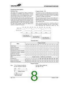
Location 018H
M
P
0
This area is reserved for the Multi-function interrupt
service program. If a timer interrupt results from a
Timer/Event Counter 2 overflow, or the real time clock
time out, or Time base time out, and if the interrupt is
enabled and the stack is not full, the program will jump
to this location and begin execution.
I
n
d
i
r
e
c
t
A
d
d
r
e
M
s
s
i
n
g
R
e
g
i
s
t
e
r
1
P
1
B
P
A
C
C
P
C
L
T
B
L
P
·
Table location
T
B
L
H
Any location in the Program Memory can be used as a
look-up table. The instructions ²TABRDC [m]² (page
specified by the TBHP) for the current page, 1
page=256 words) and ²TABRDL [m]² (the last page),
transfer the contents of the lower-order byte to the
specified data memory, and the contents of the
higher-order byte to the TBLH register. This is the Ta-
ble Higher-order byte register (08H). Only the destina-
tion of the lower-order byte in the table is well-defined,
the other bits of the table word are all transferred to
the lower portion of the TBLH. The TBLH is read only,
the higher-order byte table pointer TBHP (1FH) and
the table pointer, TBLP, is a read/write register (07H),
indicating the table location. Before accessing the ta-
ble, the location should be placed in the TBHP and
TBLP registers. All the table related instructions re-
quire 2 cycles to complete the operation. These areas
may function as a normal Program Memory depend-
ing upon the user¢s requirements.
R
T
C
C
0
0
A
B
H
H
S
T
A
T
U
S
I
N
T
C
0
0
0
C
D
H
T
M
R
0
H
H
T
M
R
0
L
0
E
H
T
T
M
M
R
R
0
1
C
H
0
F
H
H
H
H
H
H
H
H
H
H
H
1
1
1
1
1
1
1
1
1
1
0
1
2
3
4
5
6
7
8
9
T
M
R
1
L
T
M
R
1
C
P
A
P
A
C
P
B
S
p
e
c
i
a
l
P
u
r
p
o
s
e
P
B
C
D
a
t
a
M
e
m
o
r
y
P
P
C
P
P
C
D
C
C
D
1
1
A
B
H
H
P
P
P
P
W
W
W
W
M
M
M
M
0
1
2
3
1
1
C
D
H
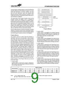
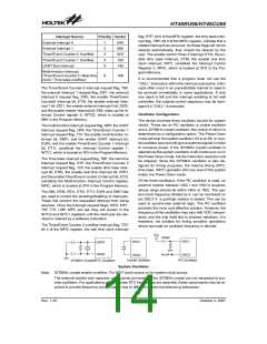
Stack Register - STACK
H
The stack register is a special part of the memory used
to save the contents of the program counter. The stack
is organized into 16 levels and is neither part of the data
nor part of the program, and is neither readable nor
writeable. Its activated level is indexed by a stack
pointer, known as SP, which is neither readable nor
writeable. At the start of a subroutine call or an interrupt
acknowledgment, the contents of the program counter
is pushed onto the stack. At the end of the subroutine or
interrupt routine, signaled by a return instruction, RET or
RETI, the contents of the program counter is restored to
its previous value from the stack. After a device reset,
the stack pointer will point to the top of the stack.
1
E
H
I
N
T
C
1
1
F
H
H
H
H
H
H
H
H
H
H
H
T
B
H
P
2
2
2
2
2
2
2
2
2
2
0
1
2
3
4
5
6
7
8
9
A
D
R
L
A
A
D
D
R
C
H
R
A
C
S
R
2
2
A
B
H
H
If the stack is full and a non-masked interrupt takes
place, the interrupt request flag is recorded but the ac-
knowledge signal is still inhibited. Once the SP is decre-
mented, using an RET or RETI instruction, the interrupt
is serviced. This feature prevents stack overflow, allow-
ing the programmer to use the structure easily. Like-
wise, if the stack is full, and a ²CALL² is subsequently
executed, a stack overflow occurs and the first entry is
lost as only the most recent 16 return addresses are
stored.
2
2
C
D
H
H
T
M
R
2
2
E
H
T
M
R
2
C
2
F
H
H
H
H
H
M
F
I
C
3
3
3
3
0
1
2
3
U
S
R
U
U
C
C
R
R
1
2
T
X
R
/
R
X
R
3
3
4
5
H
H
B
R
G
3
F
H
H
4
0
G
e
n
e
r
a
l
P
u
r
p
o
s
e
Data Memory - RAM
D
a
t
a
M
e
m
o
r
y
:
U
n
u
s
e
d
1
´
9 2 B y t e s 3
The Data Memory, RAM, has a structure of 620´8 bits,
and is divided into two functional groups, namely; spe-
cial function registers, 44´8 bits, and general purpose
data memory (Bank 0: 192´8 bits, Bank 2: 192´8 bits
(
3
B
a
n
k
s
:
B
a
n
k
0
,
B
a
n
k
2
,
B
a
n
k
3
)
R
e
a
d
a
s
"
0
0
"
F
F
H
RAM Mapping
Rev. 1.20
10
October 2, 2007

 HOLTEK [ HOLTEK SEMICONDUCTOR INC ]