HT46R064B/065B/066B
Programming Considerations
between the analog input value and the digitised output
value for the A/D converter.
When programming, special attention must be given to
the PCR[2:0] bits in the register. If these bits are all
cleared to zero no external pins will be selected for use
as A/D input pins allowing the pins to be used as normal
I/O pins. When this happens the internal A/D circuitry
will be power down. Setting the ADONB bit high has the
ability to power down the internal A/D circuitry, which
may be an important consideration in power sensitive
applications.
Note that to reduce the quantisation error, a 0.5 LSB off-
set is added to the A/D Converter input. Except for the
digitised zero value, the subsequent digitised values will
change at a point 0.5 LSB below where they would
change without the offset, and the last full scale digitised
value will change at a point 1.5 LSB below the VDD level.
A/D Programming Example
The following two programming examples illustrate how
to setup and implement an A/D conversion. In the first
example, the method of polling the EOCB bit in the
ADCR register is used to detect when the conversion
cycle is complete, whereas in the second example, the
A/D interrupt is used to determine when the conversion
is complete.
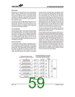
A/D Transfer Function
As the device contain a 12-bit A/D converter, its
full-scale converted digitised value is equal to FFFH.
Since the full-scale analog input value is equal to the
VDD voltage, this gives a single bit analog input value of
V
DD/4096. The diagram show the ideal transfer function
P
C
R
2
~
0
0
0
B
x
x
x
B
-
P
C
R
[
2
:
0
]
i
s
n
o
t
e
q
u
a
l
t
o
"
0
"
P
C
R
0
A
D
O
N
B
t
O
N
2
S
T
A
D
C
m
o
d
u
l
e
o
f
f
o
n
o
n
O
N
A
/
D
s
a
m
p
l
i
n
g
A
/
t
D
i
m
s
e
a
m
p
l
i
n
g
t
i
m
e
A
D
t
C
S
A
D
t
C
S
S
T
A
R
T
E
O
C
B
A
C
S
2
~
x
x
x
B
0
0
0
B
0
0
1
B
0
1
0
B
A
C
S
0
P
o
w
e
r
-
o
n
S
t
a
r
t
o
f
A
/
D
S
t
a
r
t
o
f
A
/
D
S
t
a
r
t
o
f
A
/
D
R
e
s
e
t
c
o
n
v
e
r
s
i
o
n
c
o
n
v
e
r
s
i
o
n
c
o
n
v
e
r
s
i
o
n
R
e
s
e
t
A
/
D
R
c
e
s
e
t
A
/
D
R
e
s
e
t
A
/
D
c
o
n
v
e
r
t
e
r
o
n
v
e
r
t
e
r
c
o
e
n
v
e
r
t
e
r
E
n
d
o
f
A
/
D
E
n
d
o
f
A
/
D
c
o
n
v
e
r
s
i
o
n
c
n
o
n
v
e
r
s
i
o
n
1
:
D
e
f
i
n
p
o
r
t
c
o
n
f
i
g
u
r
a
t
i
o
2
:
S
e
l
e
c
t
a
n
a
l
o
g
c
h
a
n
n
e
l
t
A
D
C
t
A
D
C
A
/
D
c
o
n
v
e
r
s
i
A
o
/
n
D
t
c
i
m
o
n
e
v
e
r
s
i
o
n
t
i
m
e
N
o
t
A
t
e
/
:
D
c
l
o
c
k
S
Y
/
m
S
2
S
u
,
Y
/
s
S
4
t
f
S
,
Y
/
b
S
8
f
S
e
,
Y
/
S
f
f
s
6
S
y
Y
/
s
o
S
3
,
r
2
f
f
A
A
D
D
=
C
C
S
4
A
D
t
t
=
A
1
D
6
t
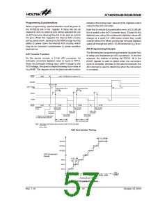
A/D Conversion Timing
1
.
5
L
S
B
F
F
F
H
F
F
E
H
F
F
D
H
A
/
D
C
o
n
v
e
r
s
i
o
n
R
e
s
u
l
t
0
.
5
L
S
B
0
0
0
3
2
1
H
H
H
V
D
D
(
)
4
0
9
6
9
0
1
2
3
4
0
4
9
0
3
9
4
4
0
9
5
4
0
6
A
n
a
l
o
g
I
n
p
u
t
V
o
l
t
a
g
e
Ideal A/D Transfer Function
Rev. 1.10
57
October 23, 2012

 HOLTEK [ HOLTEK SEMICONDUCTOR INC ]