HT46R064B/065B/066B
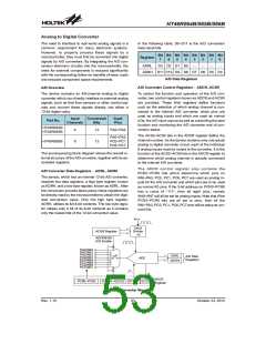
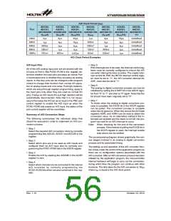
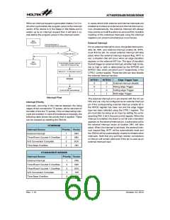
A/D Clock Period (tAD
)
ADCS2,
ADCS1,
ADCS2,
ADCS1,
ADCS2,
ADCS1,
ADCS2,
ADCS1,
ADCS2,
ADCS1,
ADCS2,
ADCS1,
ADCS2,
ADCS1,
fSYS
ADCS0=000 ADCS0=001 ADCS0=010 ADCS0=100 ADCS0=101 ADCS0=110 ADCS0=011,
(fSYS/2)
(fSYS/8)
(fSYS/32)
(fSYS)
(fSYS/4)
(fSYS/16)
16ms
8ms
111
1MHz
2MHz
4MHz
8MHz
12MHz
Undefined
Undefined
Undefined
Undefined
Undefined
2ms
8ms
32ms
1ms
4ms
500ns
250ns*
125ns*
83ns*
1ms
4ms
16ms
2ms
500ns
250ns*
167ns*
2ms
8ms
1ms
4ms
500ns
333ns*
1ms
4ms
2ms
667ns
2.67ms
1ms
A/D Clock Period Examples
·
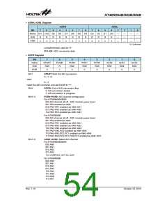
A/D Input Pins
Step 5
If the interrupts are to be used, the interrupt control reg-
isters must be correctly configured to ensure the A/D
converter interrupt function is active. The master inter-
rupt control bit, EMI, the INTC0 interrupt control regis-
ter must be set to ²1², the A/D converter interrupt bit,
ADE, must also be set to ²1².
All of the A/D analog input pins are pin-shared with the
I/O pins on Port A. Bits PCR2~PCR0 in the register, de-
termine whether the input pins are setup as normal Port
A input/output pins or whether they are setup as analog
inputs. In this way, pins can be changed under program
control to change their function from normal I/O opera-
tion to analog inputs and vice versa. Pull-high resistors,
which are setup through register programming, apply to
the input pins only when they are used as normal I/O
pins, if setup as A/D inputs the pull-high resistors will be
automatically disconnected. Note that it is not neces-
sary to first setup the A/D pin as an input in the PBC port
control register to enable the A/D input as when the
PCR2~PCR0 bits enable an A/D input, the status of the
port control register will be overridden.
·
·
Step 6
The analog to digital conversion process can now be
initialised by setting the START bit in the ADCR regis-
ter from ²0² to ²1² and then to ²0² again. Note that this
bit should have been originally set to ²0².
Step 7
To check when the analog to digital conversion pro-
cess is complete, the EOCB bit in the ADCR register
can be polled. The conversion process is complete
when this bit goes low. When this occurs the A/D data
registers ADRL and ADRH can be read to obtain the
conversion value. As an alternative method if the in-
terrupts are enabled and the stack is not full, the pro-
gram can wait for an A/D interrupt to occur.
Summary of A/D Conversion Steps
The following summarises the individual steps that
should be executed in order to implement an A/D con-
version process.
Note: When checking for the end of the conversion
process, if the method of polling the EOCB bit in
the ADCR register is used, the interrupt enable
step above can be omitted.
·
Step 1
Select the required A/D conversion clock by correctly
programming bits ADCS2, ADCS1 and ADCS0 in the
register.
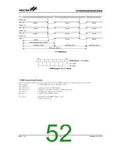
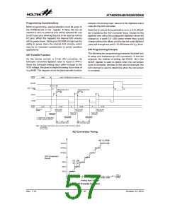
The accompanying diagram shows graphically the vari-
ous stages involved in an analog to digital conversion
process and its associated timing.
·
Step 2
Select which pins are to be used as A/D inputs and
configure them as A/D input pins by correctly pro-
gramming the PCR2~PCR0 bits in the ADCR register.
The setting up and operation of the A/D converter func-
tion is fully under the control of the application program as
there are no configuration options associated with the
A/D converter. After an A/D conversion process has been
initiated by the application program, the microcontroller
internal hardware will begin to carry out the conversion,
during which time the program can continue with other
functions. The time taken for the A/D conversion is 16tAD
where tAD is equal to the A/D clock period.
·
·
Step 3
Enable the A/D by clearing the ADONB in the ACSR
register to zero.
Step 4
Select which channel is to be connected to the internal
A/D converter by correctly programming the
ACS2~ACS0 bits which are also contained in the reg-
ister.
Rev. 1.10
56
October 23, 2012

 HOLTEK [ HOLTEK SEMICONDUCTOR INC ]