HT46F46E/HT46F47E/HT46F48E/HT46F49E
Read Only Memory, is by its nature a non-volatile form
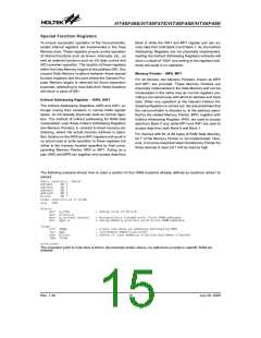
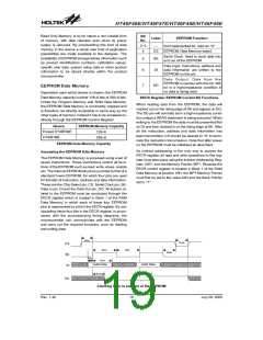
Bit
Label
EEPROM Function
No.
of memory, with data retention even when its power
supply is removed. By incorporating this kind of data
memory in the device a whole new host of application
possibilities are made available to the designer. The
availability of EEPROM storage allows information such
as product identification numbers, calibration values,
specific user data, system setup data or other product
information to be stored directly within the product
microcontroller.
0~3
4
¾
Not implemented bit, read as ²0²
CS
EEPROM Data Memory select
Serial Clock: Used to clock data into
and out of the EEPROM
5
6
SK
DI
Data Input: Instructions, address and
data information are written to the
EEPROM on this pin
Data Output: Data from the
EEPROM is readout with this bit. Will
be in a high-impedance condition if
no data is being read.
7
DO
EEPROM Data Memory
Dependent upon which device is chosen, the EEPROM
Data Memory capacity is either 128´8 bits or 256´8 bits.
Unlike the Program Memory and RAM Data Memory,
the EEPROM Data Memory is not directly mapped and
is therefore not directly accessible in same way as the
other types of memory. Instead it has to be accessed in-
directly through the EEPROM Control Register.
EECR Register EEPROM Control Bit Functions
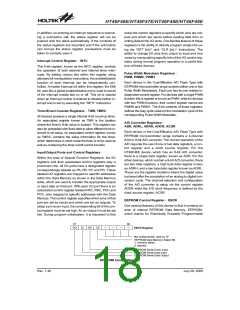
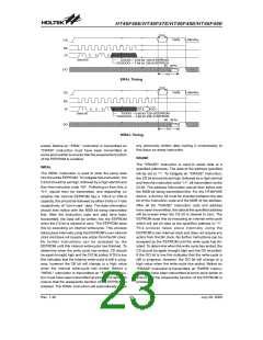
When reading data from the EEPROM, the data will
clocked out on the rising edge of SK and appear on DO.
The DO pin will normally be in a high-impedance condi-
tion unless a READ statement is being executed. When
writing to the EEPROM the data must be presented first
on DI and then clocked in on the rising edge of SK. After
all the instruction, address and data information has
been transmitted, CS should be cleared to ²0² to termi-
nate the instruction transmission. Note that after power
on the EEPROM must be initialised as described.
Device
Except HT46F49E
HT46F49E
EEPROM Memory Capacity
128´8
256´8
EEPROM Data Memory Capacity
As indirect addressing is the only way to access the
EECR register, all read and write operations to this reg-
ister must take place using the Indirect Addressing Reg-
ister, IAR1, and the Memory Pointer, MP1. Because the
EECR control register is located in Bank 1 of the RAM
Data Memory at location 40H, the MP1 Memory Pointer
must first be set to the value 40H and the Bank Pointer
set to ²1².
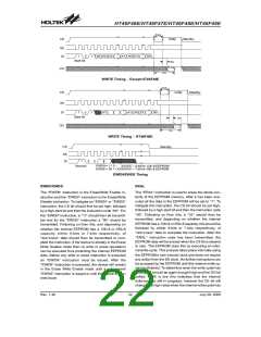
Accessing the EEPROM Data Memory
The EEPROM Data Memory is accessed using a set of
seven instructions. These instructions control all func-
tions of the EEPROM such as read, write, erase, enable
etc. The internal EEPROM structure is similar to that of a
standard 3-wire EEPROM, for which four pins are used
for transfer of instruction, address and data information.
These are the Chip Select pin, CS, Serial Clock pin, SK,
Data In pin, DI and the Data Out pin, DO. All actions re-
lated to the EEPROM must be conducted through the
EECR register which is located in Bank 1 of the RAM
Data Memory, in which each of these four EEPROM
pins is represented by a bit in the EECR register. By ma-
nipulating these four bits in the EECR register, in accor-
dance with the accompanying timing diagrams, the
microcontroller can communicate with the EEPROM
and carry out the required functions, such as reading
and writing data.
t
C
S
S
t
C
D
S
C
S
t
S
K
H
t
S
K
L
t
C
S
H
S
K
t
D
I
S
t
D
I
H
V
a
l
i
d
D
a
t
a
V
a
l
i
d
D
a
t
a
D
I
t
P
D
0
t
P
D
1
D
O
Clocking Data In and Out of the EEPROM
Rev. 1.40
19
July 28, 2009

 HOLTEK [ HOLTEK SEMICONDUCTOR INC ]