HT46F46E/HT46F47E/HT46F48E/HT46F49E
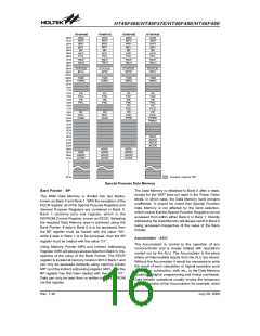
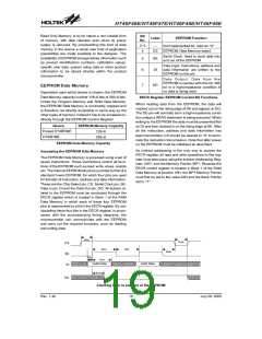
Special Function Registers
To ensure successful operation of the microcontroller,
certain internal registers are implemented in the Data
Memory area. These registers ensure correct operation
of internal functions such as timers, interrupts, etc., as
well as external functions such as I/O data control and
A/D converter operation. The location of these registers
within the Data Memory begins at the address 00H. Any
unused Data Memory locations between these special
function registers and the point where the General Pur-
pose Memory begins is reserved for future expansion
purposes, attempting to read data from these locations
will return a value of 00H.
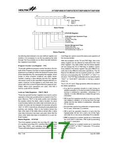
Bank 0, while the IAR1 and MP1 register pair can ac-
cess data from both Bank 0 and Bank 1. As the Indirect
Addressing Registers are not physically implemented,
reading the Indirect Addressing Registers indirectly will
return a result of ²00H² and writing to the registers indi-
rectly will result in no operation.
Memory Pointer - MP0, MP1
For all devices, two Memory Pointers, known as MP0
and MP1 are provided. These Memory Pointers are
physically implemented in the Data Memory and can be
manipulated in the same way as normal registers pro-
viding a convenient way with which to address and track
data. When any operation to the relevant Indirect Ad-
dressing Registers is carried out, the actual address that
the microcontroller is directed to, is the address speci-
fied by the related Memory Pointer. MP0, together with
Indirect Addressing Register, IAR0, are used to access
data from Bank 0 only, while MP1 and IAR1 are used to
access data from both Bank 0 and Bank 1.
Indirect Addressing Register - IAR0, IAR1
The Indirect Addressing Registers, IAR0 and IAR1, al-
though having their locations in normal RAM register
space, do not actually physically exist as normal regis-
ters. The method of indirect addressing for RAM data
manipulation uses these Indirect Addressing Registers
and Memory Pointers, in contrast to direct memory ad-
dressing, where the actual memory address is speci-
fied. Actions on the IAR0 and IAR1 registers will result in
no actual read or write operation to these registers but
rather to the memory location specified by their corre-
sponding Memory Pointer, MP0 or MP1. Acting as a
pair, IAR0 and MP0 can together only access data from
For devices with 64 or 88 bytes of RAM Data Memory,
bit 7 of the Memory Pointer is not implemented. How-
ever, it must be noted that when the Memory Pointer for
these devices is read, bit 7 will be read as high.
The following example shows how to clear a section of four RAM locations already defined as locations adres1 to
adres4.
data .section ¢data¢
adres1
adres2
adres3
adres4
block
db ?
db ?
db ?
db ?
db ?
code .section at 0 ¢code¢
org 00h
start:
mov a,04h
; setup size of block
mov block,a
mov a,offset adres1
mov mp0,a
; Accumulator loaded with first RAM address
; setup memory pointer with first RAM address
loop:
clr IAR0
inc mp0
sdz block
jmp loop
; clear the data at address defined by MP0
; increment memory pointer
; check if last memory location has been cleared
continue:
The important point to note here is that in the example shown above, no reference is made to specific RAM ad-
dresses.
Rev. 1.40
15
July 28, 2009

 HOLTEK [ HOLTEK SEMICONDUCTOR INC ]