HT46F46E/HT46F47E/HT46F48E/HT46F49E
H
T
4
6
F
4
6
H
E
T
4
6
F
4
7
H
E
T
4
6
F
4
8
H
E
T
4
6
F
4
9
E
0
0
0
0
0
0
0
0
0
0
0
1
2
3
4
5
6
7
8
9
H
H
H
H
H
H
H
H
H
H
H
H
I
A
R
0
I
A
R
0
I
I
A
A
R
R
0
1
I
I
A
A
R
R
0
1
M
P
0
M
P
0
M
M
P
P
0
1
M
M
P
P
0
1
I
A
R
1
I
A
R
1
M
P
1
M
P
1
B
P
B
P
B
P
B
P
A
C
C
A
C
C
A
C
C
A
C
C
P
C
L
P
C
L
P
C
L
P
C
L
T
B
L
P
T
B
L
P
T
B
L
P
T
B
L
P
T
B
L
H
T
B
L
H
T
B
L
H
T
B
L
H
S
T
A
T
U
S
S
T
A
T
U
S
S
T
A
T
U
S
0
0
A
B
S
T
A
T
U
S
I
N
T
C
I
N
T
C
I
N
T
C
I
N
T
C
0
0
C
D
H
H
T
M
R
T
M
R
T
M
R
T
M
R
0
E
H
H
H
H
H
H
H
H
H
H
H
H
H
H
T
M
R
C
T
M
R
C
T
M
R
C
T
M
R
C
0
F
1
1
1
1
1
1
1
1
1
1
0
1
2
3
4
5
6
7
8
9
P
P
A
B
P
P
A
B
P
P
A
B
P
P
A
B
P
P
A
B
C
C
P
P
A
B
C
C
P
P
A
B
C
C
P
P
A
B
C
C
P
P
C
D
P
P
C
D
P
P
C
D
C
C
P
P
C
D
C
C
P
D
P
D
P
D
C
P
D
C
0
1
1
A
B
P
W
M
P
W
M
P
W
M
P
W
W
M
P
M
1
1
1
C
D
H
H
1
E
H
H
H
1
F
A
D
R
L
2
0
A
D
R
H
2
H
1
A
D
C
R
2
2
2
2
2
2
2
3
4
5
6
7
H
H
H
H
H
H
A
C
S
R
A
D
R
L
A
D
R
L
A
D
R
A
D
R
H
A
D
R
H
A
D
C
R
A
D
C
R
A
D
C
R
A
C
S
R
A
C
S
R
A
C
S
R
3
F
H
:
U
n
u
s
e
d
,
r
e
a
d
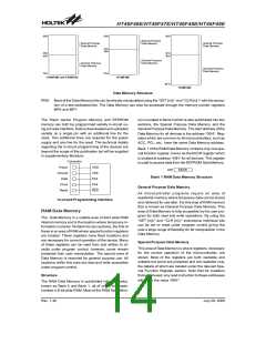
Special Purpose Data Memory
Bank Pointer - BP
The Data Memory is initialised to Bank 0 after a reset,
except for the WDT time-out reset in the Power Down
Mode, in which case, the Data Memory bank remains
unaffected. It should be noted that Special Function
Data Memory is not affected by the bank selection,
which means that the Special Function Registers can be
accessed from within either Bank 0 or Bank 1. Directly
addressing the Data Memory will always result in Bank 0
being accessed irrespective of the value of the Bank
Pointer.
The RAM Data Memory is divided into two Banks,
known as Bank 0 and Bank 1. With the exception of the
EECR register, all of the Special Purpose Registers and
General Purpose Registers are contained in Bank 0.
Bank 1 contains only one register, which is the
EEPROM Control Register, known as EECR. Selecting
the required Data Memory area is achieved using the
Bank Pointer. If data in Bank 0 is to be accessed, then
the BP register must be loaded with the value ²00²,
while if data in Bank 1 is to be accessed, then the BP
register must be loaded with the value ²01².
Accumulator - ACC
The Accumulator is central to the operation of any
microcontroller and is closely related with operations
carried out by the ALU. The Accumulator is the place
where all intermediate results from the ALU are stored.
Without the Accumulator it would be necessary to write
the result of each calculation or logical operation such
as addition, subtraction, shift, etc., to the Data Memory
resulting in higher programming and timing overheads.
Data transfer operations usually involve the temporary
storage function of the Accumulator; for example, when
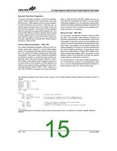
Using Memory Pointer MP0 and Indirect Addressing
Register IAR0 will always access data from Bank 0, irre-
spective of the value of the Bank Pointer. The EECR
register is located at memory location 40H in Bank 1 and
can only be accessed indirectly using memory pointer
MP1 and the indirect addressing register, IAR1, after the
BP register has first been loaded with the value ²01².
Data can only be read from or written to the EEPROM
via this register.
Rev. 1.40
16
July 28, 2009

 HOLTEK [ HOLTEK SEMICONDUCTOR INC ]