HT46R63/HT46C63
When the timer/event counter (reading TMRH) is read,
the clock will be blocked to avoid errors. As this may re-
sults in a counting error, this must be taken into consid-
eration by the programmer.
16H or 18H). For output operation, all the data is latched
and remains unchanged until the output latch is rewrit-
ten.
Each I/O line has its own control register (PAC, PBC,
PCC, PDC) to control the input/output configuration.
With this control register, CMOS output or schmitt trig-
ger input with or without (depends on options) pull-high
resistor structures can be reconfigured dynamically (i.e.,
on-the fly) under software control. To function as an in-
put, the corresponding latch of the control register has to
be set as ²1². The pull-high resistor (if the pull-high re-
sistor is enabled) will be exhibited automatically. The in-
put sources are also dependent on the control register. If
the control register bit is ²1², the input will read the pad
state (²mov² and read-modify-write instructions). If the
control register bit is ²0², the contents of the latches will
move to internal data bus (²mov² and read-modify-write
instructions). The input paths (pad state or latches) of
read-modify-write instructions are dependent on the
control register bits. For output function, CMOS is the
only configuration. These control registers are mapped
to locations 13H, 15H, 17H and 19H.
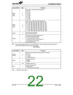
Label
Bits
Function
(TMRC)
0~2
¾
Unused bits, read as ²0²
To define the active edge of TMR pin in-
put signal
TE
3
(0=active on low to high;
1=active on high to low)
To enable or disable timer counting
(0=disabled; 1=enabled)
TON
4
5
¾
Unused bit, read as ²0²
To define the operating mode
01=Event count mode (external clock)
10=Timer mode (internal clock)
11=Pulse width measurement mode
00=Unused
TM0
TM1
6
7
TMRC Register
Input/Output Ports
After a chip reset, these input/output lines stay at a high
level (pull-high options) or floating state (non-pull-high
options). Each bit of these input/output latches can be
set or cleared by ²SET [m].i² (m=12H, 14H, 16H or 18H)
instructions. Some instructions first input data and then
follow the output operations. For example, ²SET [m].i²
CLR [m].i², ²CPLA [m]² read the entire port states into
the CPU, execute the defined operations (bit-operation),
There are 32 bi-directional input/output lines in the mi-
cro-controller, labeled from PA to PD, which are mapped
to the data memory of [12H], [14H], [16H] and [18H], re-
spectively. All of these I/O ports can be used as input
and output operations. For input operation, these ports
are non-latching, that is, the inputs must be ready at the
T2 rising edge of instruction ²MOV A,[m]² (m=12H, 14H,
V
D
D
C
o
n
t
r
o
l
B
i
t
P
H
D
Q
D
a
t
a
B
u
s
W
r
i
t
e
C
o
n
t
r
o
l
R
e
g
i
s
t
e
r
C
K
Q
S
C
h
i
p
R
e
s
e
t
P
A
0
~
P
A
7
P
B
0
~
P
B
7
P
P
C
D
0
~
P
C
7
R
e
a
d
C
o
n
t
r
o
l
R
e
g
i
s
t
e
r
0
~
P
D
7
D
a
t
a
B
i
t
D
C
Q
K
Q
W
r
i
t
e
D
a
t
a
R
e
g
i
s
t
e
r
S
P
W
M
0
~
P
W
M
3
(
P
D
0
~
P
D
3
O
n
l
y
)
M
U
X
R
e
a
d
D
a
t
a
R
e
g
i
s
t
e
r
S
y
s
t
e
m
W
a
k
e
-
u
p
W
a
k
e
-
u
p
o
p
t
i
o
n
s
(
P
A
o
n
l
y
)
P
u
l
s
e
G
e
n
e
r
a
t
o
r
T
o
I
n
t
e
r
r
u
p
t
D
i
s
a
b
l
e
/
H
i
g
h
/
L
o
w
H
i
g
h
-
L
o
w
E
d
g
e
t
o
P
u
l
s
e
P
D
4
a
n
d
P
D
5
Input/Output Ports
Rev. 1.90
18
May 17, 2004

 HOLTEK [ HOLTEK SEMICONDUCTOR INC ]