HT46R63/HT46C63
V
D
D
E
x
t
e
r
n
a
l
R
V
L
C
D
V
V
3
2
N
o
t
e
:
B
L
L
i
a
s
c
u
r
r
e
n
t
(
l
o
w
,
m
i
d
d
l
e
o
r
h
i
g
h
)
i
s
s
e
l
e
c
t
a
b
l
e
b
y
R
O
M
c
o
d
e
o
p
t
i
o
n
.
C
L
C
D
D
D
L
C
D
D
D
C
S
S
L
C
D
L
C
D
L
C
D
V
1
*
D
D
L
C
D
L
o
w
:
8
e
m
A
,
e
x
t
e
r
n
x
a
l
R
=
2
4
0
k
1
W
M
H
i
d
d
l
:
1
6
m
A
,
e
t
e
r
a
n
a
l
R
=
2
0
k
W
i
g
h
:
4
8
m
A
,
e
x
t
e
r
n
l
R
=
3
4
0
k
V
0
L
C
D
O
n
/
O
f
f
*
*
V
D
D
=
3
V
,
B
i
a
s
f
o
r
V
L
C
D
=
V
L
o
w
:
8
e
m
A
,
e
x
t
e
r
n
x
a
l
R
=
0
k
W
M
H
i
d
d
l
:
1
6
m
A
,
e
t
e
r
a
n
a
l
R
=
0
k
W
i
g
h
:
4
8
m
A
,
e
x
t
e
r
n
l
R
=
0
k
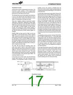
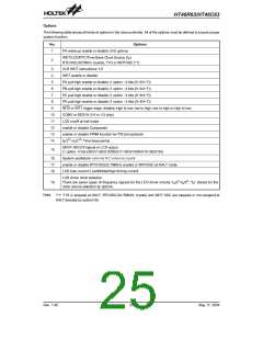
LCD Bias Block Diagram and Application Circuit
A/D Converter
channels to select. The bit5~bit3 of the ADCR are used
to set PB configurations. PB can be an analog input or
as digital I/O line decided by these 3 bits. Once a PB line
is selected as an analog input, the I/O functions and
pull-high resistor of this I/O line are disabled. The EOCB
bit (bit 6 of the ADCR) is end of A/D conversion flag.
Check this bit to know when A/D conversion is com-
pleted. The START bit of the ADCR is used to begin the
conversion of A/D converter. Give START bit a falling
edge that means the A/D conversion has started. The
A/D converter remains in reset state while the START
stays at ²1². In order to ensure the A/D conversion is
completed, the START should stay at ²0² until the
EOCB is cleared to ²0² (end of A/D conversion).
The 8 channels and 8-bit resolution (7-bit accuracy) A/D
converter are implemented in this microcontroller. The
reference voltage is AVDD. The AVDD pin must be con-
nected to VDD externally. Conversion accuracy may
therefore be degraded by voltage drops and noise in the
event of heavily loaded or badly coupled power supply
lines. The A/D converter contains 3 special registers
which are; ADR (21H), ADCR (22H) and ACSR (23H).
The ADR is A/D result register. After the A/D conversion
is completed, the ADR should be read to get the conver-
sion result data. The ADCR is an A/D converter control
register, which defines the A/D channel number, analog
channel select, start A/D conversion control bit and the
end of A/D conversion flag. If the users want to start an
A/D conversion, after select the converted analog chan-
nel, and then give START bit a positive pulse (0®1®0).
At the end of A/D conversion, the EOCB bit is cleared
and an A/D converter interrupt occurs(if the A/D con-
verter interrupt is enabled). The ACSR is an A/D clock
setting register, which is used to select the A/D clock
source.
The bit 7 of the ACSR is used for testing purpose only. It
can not be used for the users. The bit1 and bit0 of the
ACSR are used to select A/D clock sources.
When the A/D conversion is completed, the A/D inter-
rupt request flag is set. The bit is set to ²1² when the
START bit is set to ²1².
Register Bit7 Bit6 Bit5 Bit4 Bit3 Bit2 Bit1 Bit0
The A/D converter control register is used to control the
A/D converter. The bit2~bit0 of the ADCR are used to
select an analog input channel. There are a total of 8
ADR
D7 D6 D5 D4 D3 D2 D1 D0
Rev. 1.90
21
May 17, 2004

 HOLTEK [ HOLTEK SEMICONDUCTOR INC ]