HT45R37
Buzzer
Operating in a similar way to the Programmable Fre-
quency Divider, the Buzzer function provides a means of
producing a variable frequency output, suitable for ap-
plications such as Piezo-buzzer driving or other external
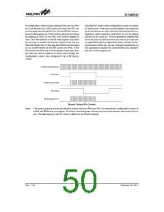
circuits that require a precise frequency generator.
that generates fS, which in turn controls the buzzer fre-
quency, can originate from three different sources, the
32768Hz oscillator, the 32K_INT oscillator or the Sys-
tem oscillator/4, the choice of which is determined by
the fS clock source configuration option. Note that the
buzzer frequency is controlled by configuration options,
which select both the source clock for the internal clock
fS and the internal division ratio. There are no internal
registers associated with the buzzer frequency.
Buzzer Operation
The BZ and BZ pins form a complementary pair, and are
pin-shared with I/O pins, PA0 and PA1. A configuration
option is used to select from one of three buzzer options.
The first option is for both pins PA0 and PA1 to be used
as normal I/Os, the second option is for both pins to be
configured as BZ and BZ buzzer pins, the third option
selects only the PA0 pin to be used as a BZ buzzer pin
with the PA1 pin retaining its normal I/O pin function.
Note that the BZ pin is the inverse of the BZ pin which to-
gether generate a differential output which can supply
more power to connected interfaces such as buzzers.
If the configuration options have selected both pins PA0
and PA1 to function as a BZ and BZ complementary pair
of buzzer outputs, then for correct buzzer operation it is
essential that both pins must be setup as outputs by set-
ting bits PAC0 and PAC1 of the PAC port control register
to zero. The PA0 data bit in the PA data register must
also be set high to enable the buzzer outputs, if set low,
both pins PA0 and PA1 will remain low. In this way the
single bit PA0 of the PA register can be used as an on/off
control for both the BZ and BZ buzzer pin outputs. Note
that the PA1 data bit in the PA register has no control
over the BZ buzzer pin PA1.
The buzzer is driven by the internal clock source, , which
then passes through a divider, the division ratio of which
is selected by configuration options to provide a range of
buzzer frequencies from fS/22 to fS/29. The clock source
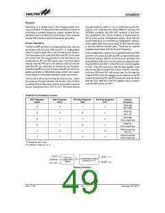
PA0/PA1 Pin Function Control
PAC Register
PAC0
PAC Register
PAC1
PA Data Register
PA0
PA Data Register
PA1
Output
Function
PA0=BZ
PA1=BZ
0
0
0
0
1
1
0
0
1
1
0
1
1
0
1
0
x
x
x
x
PA0=²0²
PA1=²0²
PA0=BZ
x
PA1=input line
PA0=²0²
x
PA1=input line
PA0=input line
PA1=D
D
x
PA0=input line
PA0=input line
²x² stands for don¢t care
²D² stands for Data ²0² or ²1²
f
S
Y
S
B
B
Z
Z
f
S
S
o
u
r
c
e
f
S
C
o
n
f
i
g
u
r
a
t
i
o
n
O
p
t
i
o
n
3
2
7
6
8
C
H
o
z
n
f
i
g
u
r
a
t
i
o
n
2
d
9
D
i
v
i
~
e
2
b
y
2
O
p
t
i
o
n
3
2
K
_
I
N
T
Buzzer Function
Rev. 1.20
49
February 25, 2011
图片预览")
 HOLTEK [ HOLTEK SEMICONDUCTOR INC ]