HT45R37
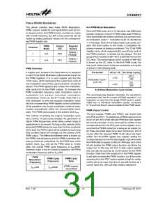
The values in Timer A and Timer B is changed by writing
to the high byte registers, TMRAH and TMRBH, but writ-
ing to the low byte registers TMRAL and TMRBL will
keep the values in Timer A and Timer B unchanged.
Reading registers TMRAH and TMRBH will also latch
the TMRAL TMRBL values into the low byte buffer to
avoid false timing problems. Reading from registers
TMRAL and TMRBL returns the contents of the low byte
buffer only. Therefore, the low byte of Timer A and Timer
B cannot be read directly. TMRAH and TMRBH must be
read first to ensure that the low byte contents of Timer A
and Timer B are latched into the buffer.
tion. This enables applications such as multi-channel or
matrix touch switch applications to be implemented. The
bits in the ASCR0~ASCR1 registers select which of the
16-channels is to be connected to the internal C/R to F
converter. The bits in the ASCR2 register selects what
happens to the channel when the channel is inactive.
When a channel is inactive it can be selected to be
pulled low to ground or not using bits in the ASCR2 reg-
ister. As there are only 8-bits to control 16-channels the
function is selected in channel pairs. There are configu-
ration options which must first be selected to choose
which pins are to be used as inputs to the C/R to F con-
verter.
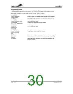
The external resistor and capacitor, together with inter-
nal inverters, form an oscillation circuit which is the clock
source for Timer B and therefore the input to registers
TMRBL and TMRBH. The RCOM0, RCOM1 and
RCOM2 bits of RCOCCR define the clock source of
Timer A.
If the configuration options have selected PA0~PA7 to
be normal I/O pins, then the corresponding bit 0~bit7
bits in the ASCR0 register will have no function and will
be read as zero. Similarly if the configuration options
have selected PD0~PD7 to be normal I/O pins, then the
corresponding bit 0~bit7 bits in the ASCR1 register will
have no function and will be read as zero.
If the RCOCON bit in the RCOCCR register is set high,
Timer A and Timer B will start counting until either Timer
Aor Timer B overflows. The relevant Timer will then gen-
erate an interrupt request flag which is the RCOCF bit in
the INTC1 register. Timer A and Timer B will stop count-
ing and will also reset the RCOCON bit to zero at the
same time. If the RCOCON bit is set high, then the
TMRAL/TMRAH and TMRBL/TMRBH register cannot
be read or written to.
If the configuration options have selected PA0~PA7 to
be normal I/O pins, then the corresponding bits in the
ASCR2 register, bit 0 ~ bit3, must be cleared to zero to
disable the RC0/RC1, RC2/RC3, RC4/RC5 and RC6/RC7
pull-low resistors. Similarly if the configuration options
have selected PD0~PD7 to be normal I/O pins, then the
corresponding bits in the ASCR2 register, bit 4~bit7, must
be cleared to zero to disable the RC8/RC9, RC10/RC11,
RC12/RC13 or RC14/RC15 pull-low resistors.
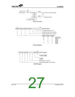
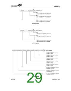
C/R to F Converter Analog Switches
The device contains only one internal C/R to F converter
function, however it can be connected to any of the 16
external channels using its internal analog switch func-
R
e
g
i
s
t
e
r
s
M
C
U
A
A
A
S
S
S
C
C
C
R
R
R
0
1
2
A
.
S
.
0
~
A
.
S
.
1
R
C
0
~
R
C
1
5
A
S
C
R
0
/
A
S
C
R
E
x
t
e
r
n
a
l
R
C
R
e
g
i
s
t
e
r
C
o
A
n
a
l
o
g
R
R
C
C
0
1
A
A
.
.
S
S
.
.
0
S
w
i
t
c
h
e
s
R
C
0
~
R
C
1
5
1
P
u
l
l
-
l
o
w
A
S
C
R
2
R
e
g
i
s
t
e
r
C
o
n
R
R
C
C
1
1
4
5
A
A
.
.
S
S
.
.
1
1
4
5
A
n
a
S
l
w
o
i
g
t
c
h
R
C
O
U
T
/
I
N
T
i
m
e
r
B
C
l
o
c
k
S
o
u
r
c
e
R
C
R
R
E
E
F
F
Analog Switches and C/R to F Oscillator
Rev. 1.20
28
February 25, 2011
图片预览")
 HOLTEK [ HOLTEK SEMICONDUCTOR INC ]