HT45R37
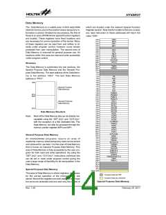
Data Memory
The Data Memory is a volatile area of 8-bit wide RAM
internal memory and is the location where temporary in-
formation is stored. Divided into two sections, the first of
these is an area of RAM where special function registers
are located. These registers have fixed locations and
are necessary for correct operation of the device. Many
of these registers can be read from and written to di-
rectly under program control, however, some remain
protected from user manipulation. The second area of
Data Memory is reserved for general purpose use. All
locations within this area are read and write accessible
under program control.
which are located under the relevant Special Function
Register section. Note that for locations that are unused,
any read instruction to these addresses will return the
value ²00H².
0
0
0
0
0
0
0
0
0
0
0
1
2
3
4
5
6
7
8
9
H
H
H
H
H
H
H
H
H
H
I
A
R
0
M
P
0
I
A
R
1
M
P
1
A
C
C
P
C
L
T
B
L
P
T
B
T
L
H
R
C
C
0
0
A
B
H
H
H
H
H
H
S
T
A
T
U
S
I
N
T
C
0
Structure
0
0
C
D
T
M
R
0
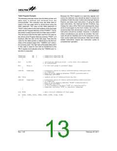
The Data Memory is subdivided into two sections, the
Special Purpose Data Memory and the General Pur-
pose Data Memory. The start address of the Data Mem-
ory is the address ²00H². The last Data Memory
address is ²FFH².
0
E
T
M
R
0
C
0
1
2
3
F
F
F
F
1
1
1
1
1
1
1
1
1
1
0
1
2
3
4
5
6
7
8
9
H
H
H
H
H
H
H
H
H
H
P
P
A
B
P
P
A
B
C
C
0
0
H
P
P
C
D
P
P
C
D
C
C
S
D
p
e
c
i
a
l
P
u
a
t
a
M
e
m
o
1
1
A
B
H
H
H
H
H
H
P
P
W
W
M
M
0
1
L
L
5
F
H
H
P
P
W
W
M
M
0
1
H
H
6
0
1
1
C
D
1
E
I
N
T
C
1
G
D
e
n
e
r
a
l
P
a
t
a
M
e
m
o
M
M
F
F
0
I
C
2
0
H
I
C
1
2
H
1
A
A
A
S
S
S
C
C
C
R
R
R
0
1
2
F
F
H
2
2
2
2
2
2
2
2
2
3
4
5
6
7
8
9
H
H
H
H
H
H
H
H
Data Memory Structure
A
D
R
L
A
D
R
C
H
Note: Most of the Data Memory bits can be directly ma-
nipulated using the ²SET [m].i² and ²CLR [m].i²
with the exception of a few dedicated bits. The
Data Memory can also be accessed through the
memory pointer registers MP0 and MP1.
A
D
R
A
C
S
R
C
L
K
M
O
D
P
A
W
U
2
2
A
B
H
H
H
H
H
H
P
P
A
P
P
U
B
U
2
2
C
D
P
P
C
D
P
P
U
U
2
E
I
N
T
E
D
G
E
General Purpose Data Memory
M
I
S
C
3
3
3
3
3
3
3
3
3
3
0
1
2
3
4
5
6
7
8
9
H
H
H
H
H
H
H
H
H
H
T
T
M
M
R
R
A
B
H
H
All microcontroller programs require an area of
read/write memory where temporary data can be stored
and retrieved for use later. It is this area of Data Memory
that is known as General Purpose Data Memory. This
area of Data Memory is fully accessible by the user pro-
gram for both read and write operations. By using the
²SET [m].i² and ²CLR [m].i² instructions individual bits
can be set or reset under program control giving the
user a large range of flexibility for bit manipulation in the
Data Memory.
T
T
M
M
R
R
A
B
L
L
R
C
O
C
C
R
R
C
O
C
R
S
I
M
C
T
L
0
1
S
I
M
C
T
L
S
I
M
D
R
S
I
M
A
R
/
S
I
M
C
T
L
2
3
3
A
B
H
H
H
H
H
H
T
M
R
1
T
M
R
1
C
3
3
C
D
3
E
Special Purpose Data Memory
4
0
H
~
5
H
F
This area of Data Memory is where registers, necessary
for the correct operation of the microcontroller, are
stored. Most of the registers are both read and write type
but some are protected and are read only, the details of
:
:
U
U
n
n
u
u
s
e
d
r
r
e
a
d
a
a
s
s
s
e
d
e
a
d
Special Purpose Data Memory
Rev. 1.20
14
February 25, 2011
图片预览")
 HOLTEK [ HOLTEK SEMICONDUCTOR INC ]