Preliminary
HT45R04/HT45R04E
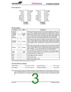
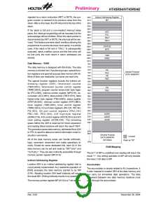
Pin Assignment
P
A
3
/
P
F
D
P
A
4
/
T
I
M
R
P
A
3
/
P
F
D
P
P
A
A
4
5
/
T
M
R
1
2
3
4
5
6
7
8
9
1
1
1
1
1
1
1
1
1
8
7
6
5
4
3
2
1
0
1
2
3
4
5
6
7
8
9
1
1
1
1
1
1
1
1
1
8
7
6
5
4
3
2
1
0
P
A
2
P
A
5
/
N
T
P
A
2
/
I
N
T
P
P
A
A
1
0
P
A
A
6
7
P
P
A
A
1
0
P
A
6
P
P
O
A
7
/
S
D
A
P
P
P
P
B
B
B
B
3
2
1
0
/
/
/
/
A
A
A
A
N
N
N
N
3
2
1
0
O
O
S
C
2
1
P
P
B
B
3
2
/
/
A
A
N
N
3
2
S
C
2
1
S
C
O
S
C
V
D
D
P
B
1
/
A
N
1
V
D
D
P
B
0
/
A
N
0
R
P
E
S
R
P
E
S
V
S
S
D
0
V
S
S
D
0
/
S
C
L
H
T
4
5
R
0
4
H
T
4
5
R
0
4
E
1
8
S
O
P
-
A
1
8
S
O
P
-
B
Pin Description
Pin Name
I/O
Option
Description
PA0~PA2
PA3/PFD
PA4/TMR
PA5/INT
PA6
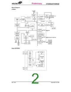
Bidirectional 8-bit input/output port. Each bit can be configured as a wake-up in-
put by options. Software instructions determine the CMOS output or Schmitt
trigger input with pull-high resistors (determined by pull-high option: bit option).
The I/O modes of each line are controlled by their related control register bit
(PAC). The PA3, PA4 and PA5 are pin-shared with PFD, TMR and INT , re-
spectively. PA7/SDA is wire-bonded with SDA pad of the data EEPROM.
Pull-high
Wake-up
PFD
I/O
PA7/SDA
Bidirectional 4-bit input/output port. Software instructions determine the CMOS
output or Schmitt trigger input with pull-high resistors (determined by pull-high
option: bit option). The I/O modes of each line are controlled by their related
control register bit (PBC). Each PB line is pin shared with an A/D converter in-
put.
PB0/AN0~
PB3/AN3
I/O
I/O
Pull-high
Pull-high
Bidirectional 1-bit input/output port. Software instructions determine the CMOS
output or Schmitt trigger input with pull-high resistors (determined by pull-high
option: bit option). The I/O mode is controlled by its related control register bit
(PDC). PDO/SCL is wire-bonded with SCL pad of the data EEPROM.
PD0/SCL
OSC1 and OSC2 are connected to an RC network or a crystal (determined by
options) for the internal system clock. In the case of an RC operation, OSC2 is
the output terminal for 1/4 system clock.
OSC1
OSC2
I
Crystal
or RC
O
RES
VDD
VSS
Schmitt trigger reset input. Active low.
Positive power supply
¾
¾
¾
¾
¾
¾
Negative power supply, ground.
Note: All pull-high resistors are controlled by an option bit.
Absolute Maximum Ratings
Supply Voltage...........................VSS-0.3V to VSS+6.0V
Input Voltage..............................VSS-0.3V to VDD+0.3V
Storage Temperature............................-50°C to 125°C
Operating Temperature...........................-40°C to 85°C
Note: These are stress ratings only. Stresses exceeding the range specified under ²Absolute Maximum Ratings² may
cause substantial damage to the device. Functional operation of this device at other conditions beyond those
listed in the specification is not implied and prolonged exposure to extreme conditions may affect device reliabil-
ity.
Rev. 0.00
3
December 30, 2004

 HOLTEK [ HOLTEK SEMICONDUCTOR INC ]