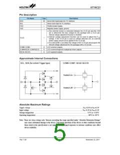
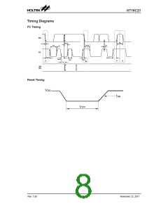
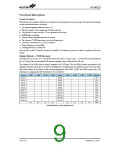
HT16C21
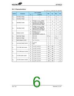
A.C. Characteristics
VSS = 0V; VDD = 2.4 to 5.5V; Ta =-40~85°C
Test Condition
Condition
Symbol
Parameter
Min.
Typ.
Max.
Unit
VDD
fLCD1
fLCD2
fLCD3
fLCD4
tOFF
LCD Frame Frequency
LCD Frame Frequency
LCD Frame Frequency
LCD Frame Frequency
VDD Off Times
4V 1/4duty, Ta =25°C
72
144
52
80
160
80
88
176
124
248
—
Hz
Hz
4V 1/4duty, Ta =25°C
4V 1/4duty, Ta=- 40 to +85°C
4V 1/4duty, Ta=-40 to +85°C
Hz
104
20
160
—
Hz
—
—
VDD drop down to 0V
—
ms
tSR
VDD Slew Rate
0.05
—
—
V/ms
Note: 1. If the conditions of Power on Reset timing are not satisfied during the power ON/OFF sequence, the
internal Power on Reset (POR) circuit will not operate normally.
2. If the VDD voltage drops below the minimum voltage of operating voltage spec. during operating, the
Power on Reset timing conditions must also be satisfied. That is, the VDD voltage must drop to 0V and
remain at 0V for 20ms (min.) before rising to the normal operating voltage.
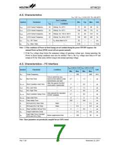
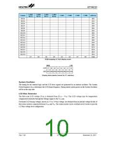
A.C. Characteristics – I2C Interface
VDD=2.4V to 5.5V VDD=3.0V to 5.5V
Symbol
fSCL
Parameter
Clock Frequency
Condition
Unit
kHz
μs
Min.
Max.
Min.
Max.
—
—
100
—
400
Time in which the bus
must be free before a new
transmission can start
tBUF
Bus Free Time
4.7
4
—
—
1.3
0.6
—
—
After this period, the first
clock pulse is generated
tHD: STA
Start Condition Hold Time
μs
tLOW
tHIGH
SCL Low Time
SCL High Time
—
—
4.7
4
—
—
1.3
0.6
—
—
μs
μs
Only relevant for repeated
START condition
tSU: STA
Start Condition Setup Time
4.7
—
0.6
—
μs
tHD: DAT
tSU: DAT
tR
Data Hold Time
—
—
0
250
—
—
4
—
—
1
0
100
—
—
—
ns
ns
μs
μs
μs
μs
Data Setup Time
SDA and SCL Rise Time
SDA and SCL Fall Time
Stop Condition Set-up Time
Output Valid from Clock
Note
Note
—
0.3
0.3
—
tF
0.3
—
3.5
—
tSU: STO
tAA
0.6
—
—
—
0.9
Input Filter Time Constant
(SDA and SCL Pins)
tSP
Noise suppression time
—
100
—
50
ns
Note: These parameters are periodically sampled but not 100% tested.
Rev. 1.00
7
November 22, 2011

 HOLTEK [ HOLTEK SEMICONDUCTOR INC ]