HT16C21
Functional Description
Power-On Reset
When the power is applied, the device is initialized by an internal power-on reset circuit. The status of the internal
circuits after initialization is as follows:
All common/segment outputs are set to VLCD
.
●
●
●
●
●
●
●
●
●
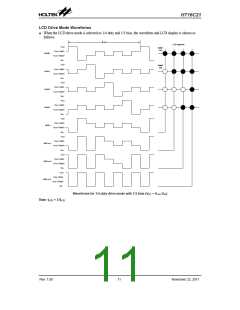
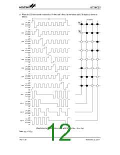
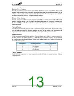
The drive mode 1/4 duty output and 1/3 bias is selected.
The System Oscillator and the LCD bias generator are off state.
LCD Display is off state.
Internal voltage adjustment function is enabled.
The Segment / VLCD shared pin is set as the Segment pin.
Detection switch for the VLCD pin is disabled.
Frame Frequency is set to 80Hz.
Blinking function is switched off.
Data transfers on the I2C interface should be avoided for 1 ms following power-on to allow completion of the reset
action.
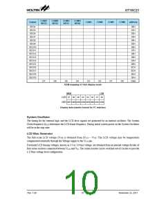
Display Memory – RAM Structure
The display RAM is static 16 x 8-bits RAM which stores the LCD data. Logic “1” in the RAM bit-map indicates
the “on” state of the corresponding LCD segment; similarly, logic 0 indicates the ‘off’ state.
The contents of the RAM data are directly mapped to the LCD data. The first RAM column corresponds to the
segments operated with respect to COM0. In multiplexed LCD applications the segment data of the second, third
and fourth column of the display RAM are time-multiplexed with COM1, COM2 and COM3 respectively. The
following is a mapping from the RAM data to the LCD pattern:
Output
SEG1
COM3
COM2
COM1
COM0
Output
SEG0
COM3
COM2
COM1
COM0 Address
00H
01H
02H
03H
04H
05H
06H
07H
08H
09H
SEG3
SEG2
SEG5
SEG4
SEG7
SEG6
SEG9
SEG8
SEG11
SEG13
SEG15
SEG17
SEG19
SEG10
SEG12
SEG14
SEG16
SEG18
D7
D6
D5
D4
D3
D2
D1
D0
Data
RAM mapping of 20x4 display mode
Rev. 1.00
9
November 22, 2011

 HOLTEK [ HOLTEK SEMICONDUCTOR INC ]