HT16C21
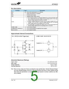
Pin Description
Pin Name
Type
Description
SDA
SCL
VDD
VSS
I/O Serial data input/output for I2C interface
I
Serial clock input for I2C interface
Positive power supply.
—
—
Negative power supply, ground.
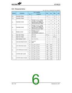
● One external resistor is connected between the VLCD pin and the VDD
pin to determine the bias voltage for the package with a VLCD pin.
Internal voltage adjustment function is disabled.
● Internal voltage adjustment function can be used to adjust the VLCD
voltage. If the VLCD pin is used as voltage detection pin, an external
power supply should not be applied to the VLCD pin.
VLCD
—
● An external MCU can detect the voltage of the VLCD pin and program the
internal voltage adjustment for the packages with a VLCD pin.
COM0~COM3
O
O
O
LCD common outputs.
COM4/SEG0~COM7/SEG3
SEG4~SEG19
LCD common/segment multiplexed driver outputs
LCD segment outputs.
Approximate Internal Connections
SCL, SDA (for schmit Trigger type)
COM0~COM7; SEG0~SEG19
Vselect-on
VDD
Vselect-off
VSS
Absolute Maximum Ratings
Supply voltage ......................................................................................................................VSS 0.3V to V +6.5V
−
SS
Input voltage ........................................................................................................................VSS 0.3V to VDD+0.3V
−
Storage temperature .......................................................................................................................-55°C to +150°C
Operating temperature .....................................................................................................................-40°C to +85°C
Note: These are stress ratings only. Stresses exceeding the range specified under "Absolute Maximum Ratings"
may cause substantial damage to the device. Functional operation of this device at other conditions beyond
those listed in the specification is not implied and prolonged exposure to extreme conditions may affect
device reliability.
Rev. 1.00
5
November 22, 2011

 HOLTEK [ HOLTEK SEMICONDUCTOR INC ]