HT16C21
Pad assignment for COB
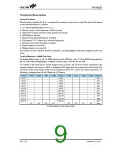
1
31 30 29 28 27 26 25 24 23 22
21
20
19
18
SEG14
SEG13
SEG12
SEG11
N.C.
2
COM0
3
4
(0, 0)
COM1
COM2
COM3
5
6
7
8
9 10 11 12 13 14 15 16 17
Chip size: 1200 x 1846μm2
Note: 1. The IC substrate should be connected to VSS in the PCB layout artwork.
2. VDD (Pad29) and VCCA2 (Pad28) must be bonded together.
3. VLCD (Pad27) and SEG19 (Pad26) must be bonded together.
Pad Coordinates for COB
Unit: μm
Y
No
1
Name
VSS
X
Y
819.9
351.435
134.752
49.752
-35.248
-120.248
-825
No
17
18
19
20
21
22
23
24
25
26
27
28
29
30
31
Name
SEG10
SEG11
SEG12
SEG13
SEG14
SEG15
SEG16
SEG17
SEG18
SEG19
VLCD
X
-423.6
-251.74
-502
426.1
502
-825
2
N.C.
279.599
364.599
449.599
534.599
819.9
3
COM0
502
4
COM1
-502
502
5
COM2
-502
502
6
COM3
-502
426.4
341.4
256.4
171.4
86.4
7
COM4/SEG0
COM5/SEG1
COM6/SEG2
COM7/SEG3
SEG4
-426.4
-341.4
-256.4
-171.4
-83.9
1.1
819.9
8
-825
819.9
9
-825
819.9
10
11
12
13
14
15
16
-825
819.9
-825
1.4
819.9
SEG5
-825
VCCA2
VDD
-83.6
-168.6
-253.6
-338.6
819.9
SEG6
86.1
-825
819.9
SEG7
171.1
256.1
341.1
-825
SDA
819.9
SEG8
-825
SCL
819.9
SEG9
-825
Rev. 1.00
4
November 22, 2011

 HOLTEK [ HOLTEK SEMICONDUCTOR INC ]