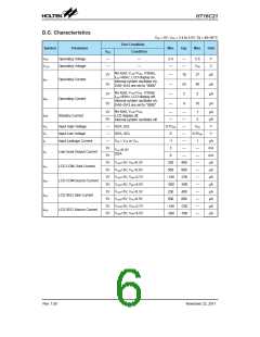
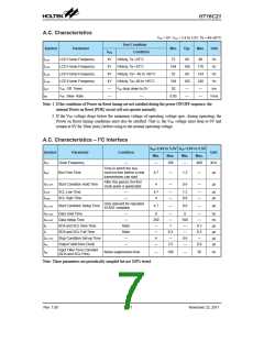
HT16C21
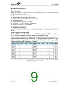
COM7/
SEG3
COM6/
SEG2
COM5/
SEG1
COM4/
SEG0
Output
COM3
COM2
COM1
COM0
address
SEG4
SEG5
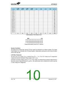
00H
01H
02H
03H
04H
05H
06H
07H
08H
09H
0AH
0BH
0CH
0DH
0EH
0FH
Data
SEG6
SEG7
SEG8
SEG9
SEG10
SEG11
SEG12
SEG13
SEG14
SEG15
SEG16
SEG17
SEG18
SEG19
D7
D6
D5
D4
D3
D2
D1
D0
RAM mapping of 16x8 display mode
MSB
LSB
D7
D6
D5
D4
D3
D2
D1
D0
LCD
LED
LED7 LED6 LED5 LED4 LED3 LED2 LED1 LED0
Display data transfer format for I2C interface
System Oscillator
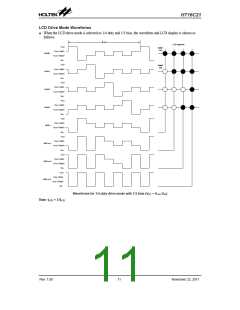
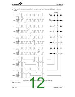
The timing for the internal logic and the LCD drive signals are generated by an internal oscillator. The System
Clock frequency (fSYS) determines the LCD frame frequency. During initial system power on the System Oscillator
will be in the stop state.
LCD Bias Generator
The full-scale LCD voltage (VOP) is obtained from (VLCD – VSS). The LCD voltage may be temperature
compensated externally through the Voltage supply to the VLCD pin.
Fractional LCD biasing voltages, known as 1/3 or 1/4 bias voltage, are obtained from an internal voltage divider of
four series resistors connected between VLCD and VSS. The centre resistor can be switched out of circuits to provide
a 1/3bias voltage level configuration.
Rev. 1.00
10
November 22, 2011

 HOLTEK [ HOLTEK SEMICONDUCTOR INC ]