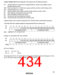
Notes: 1. In this sample program, the stack pointer (SP) is set at address H'FF80. As the stack
area, on-chip RAM addresses H'FF7E and H'FF7F are used. Therefore, when executing
this sample program, addresses H'FF7E and H'FF7F should not be used. In addition,
the on-chip RAM should not be disabled.
2. In this sample program, the program written in a ROM area (including external space)
is transferred into the RAM area and executed in the RAM to which the program is
transferred. #RAMSTR in the program is the starting destination address in RAM to
which the program is transferred. #RAMSTR must be set to an even number.
3. When executing this sample program in the on-chip ROM area or external space,
#RAMSTR should be set to #START.
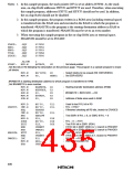
FLMCR:
EBR1:
EBR2:
TCSR:
STACK:
.RQU
.EQU
.EQU
.EQU
.EQU
H'FF80
H'FF82
H'FF83
H'FFA8
H'FF80
.ALIGN
MOV.W
2
START:
#STACK,
SP
; Set stack pointer
; Set the bits in R0 following the description on the previous page. This program is a sample program to erase
; all blocks.
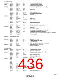
MOV.W
MOV.W
#H'0FFF, R0
R0, @EBR1
; Select blocks to be erased (R0: EBR1/EBR2)
; Set EBR1/EBR2
; #RAMSTR is starting destination address to which program is transferred in RAM.
; Set #RAMSTR to even number.
MOV.W
MOV.W
ADD.W
MOV.W
SUB.W
#RAMSTR, R2
#ERVADR, R3
; Starting transfer destination address (RAM)
;
; #RAMSTR + #ERVADR → R2
;
R3,
R2
R3
R2
#START,
R3,
; Address of data area used in RAM
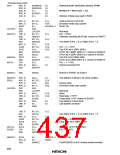
MOV.B
PRETST: CMP.B
#H'00,
#H'0C,
ERASES
#H'08,
EBR2PW
R1L,
#H'08,
R1H,
PREWRT
PWADD1
R1L,
R1L
R1L
: Used to test R1L bit in R0
; R1L = H'0C?
; If finished checking all R0 bits, branch to ERASES
;
; Test EBR1 if R1L ≥ 8, or EBR2 if R1L < 8
;
; R1L – 8 → R1H
; Test R1H bit in EBR1 (R0H)
; If R1H bit in EBR1 (R0H) is 1, branch to PREWRT
; If R1H bit in EBR1 (R0H) is 0, branch to PWADD1
; Test R1L bit in EBR2 (R0L)
; If R1L bit in EBR2 (R0H) is 1, branch to PREWRT
; R1L + 1 → R1L
BEQ
CMP.B
BMI
MOV.B
SUBX
BTST
BNE
BRA
R1L
R1H
R1H
R0H
EBR2PW: BTST
BNE
PWADD1: INC
MOV.W
R0L
R3
PREWRT
R1L
@R2+,
PRETST
; Dummy-increment R2
;
BRA
406

 HITACHI [ HITACHI SEMICONDUCTOR ]