addition, make sure that VPP is not released or shut off while the boot program is executing or
the flash memory is being programmed or erased.*1
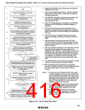
Boot mode can be released by driving the reset pin low, waiting at least ten system clock
cycles, then releasing the application of 12 V to the MD1 and FVPP pins and releasing the reset.
The settings of external pins must not change during operation in boot mode.
During boot mode, if input of 12 V to the MD1 pin stops but no reset input occurs at the RES
pin, the boot mode state is maintained within the chip and boot mode continues (but do not
stop applying 12 V to the FVPP pin during boot mode*1).
If a watchdog timer reset occurs during boot mode, this does not release the internal mode
state, but the internal boot program is restarted.
Therefore, to change from boot mode to another mode, the boot-mode state within the chip
must be released by a reset input at the RES pin before the mode transition can take place.
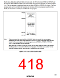
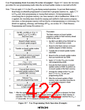
7. If the input level of the MD1 pin is changed during a reset (e.g., from 0 V to 5 V then to 12 V
while the input to the RES pin is low), the resultant switch in the microcontroller’s operating
mode will affect the bus control output signals (AS, RD, and WR) and the status of ports that
can be used for address output*2.
Therefore, either set these pins so that they do not output signals during the reset, or make sure
that their output signals do not collide with other signals outside the microcontroller.
8. When applying 12 V to the MD1 and FVPP pins, make sure that peak overshoot does not exceed
the rated limit of 13 V.
Also, be sure to connect a decoupling capacitor to the FVPP and MD1 pins.
Notes: *1 For details on applying, releasing, and shutting off VPP, see note (5) in section 19.7,
Flash Memory Programming and Erasing Precautions.
*2 These ports output low-level address signals if the mode pins are set to mode 1 during
the reset. In all other modes, these ports are in the high-impedance state. The bus
control output signals are high if the mode pins are set for mode 1 or 2 during the reset.
In mode 3, they are at high impedance.
391

 HITACHI [ HITACHI SEMICONDUCTOR ]