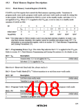
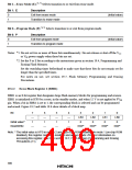
Bit 1—Erase Mode (E):*1, *2 Selects transition to or exit from erase mode.
Bit 1: E
Description
0
1
Exit from erase mode
Transition to erase mode
(Initial value)
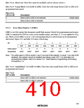
Bit 0—Program Mode (P):*1, *2 Selects transition to or exit from program mode.
Bit 0: P
Description
0
1
Exit from program mode
Transition to program mode
(Initial value)
Notes: *1 Do not set two or more of these bits simultaneously. Do not release or shut off the VCC
or VPP power supply when these bits are set.
*2 Set the P or E bit according to the instructions given in section 19.4, Programming and
Erasing Flash Memory.
Set the watchdog timer beforehand to make sure that these bits do not remain set for
longer than the specified times.
For notes on use, see section 19.7, Flash Memory Programming and Erasing
Precautions.
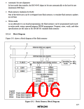
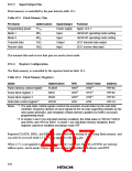
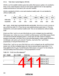
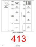
19.2.2 Erase Block Register 1 (EBR1)
EBR1 is an 8-bit register that designates large flash-memory blocks for programming and erasure.
EBR1 is initialized to H'F0 by a reset, in the standby modes, and when 12 V is not applied to FVPP
pin. When a bit in EBR1 is set to 1, the corresponding block is selected and can be programmed
and erased. Figure 19.2 and table 19.6 show details of a block map.
Bit
7
—
1
6
—
1
5
—
1
4
—
1
3
LB3
0
2
1
0
LB2LB1
0
LB0
Initial value*
0
0
Read/Write
—
—
—
—
R/W*
R/W*
R/W*
R/W*
Note: * The initial value is H'F0 in modes 2 and 3 (on-chip ROM enabled). In mode 1 (on-chip ROM
disabled), this register cannot be modified and always reads H'FF. For information on
accessing this register, refer to in section 19.7, Flash Memory Programming and Erasing
Precautions (11).
380

 HITACHI [ HITACHI SEMICONDUCTOR ]