•
•
•
Automatic bit-rate alignment
In boot-mode data transfer, the H8/3434F aligns its bit rate automatically to the host bit rate
(maximum 9600 bps).
Flash memory emulation by RAM
Part of the RAM area can be overlapped onto flash memory, to emulate flash memory updates
in real time.
Writer mode
As an alternative to on-board programming, the flash memory can be programmed and erased
in writer mode, using a general-purpose PROM programmer. Program, erase, verify, and other
specifications are the same as for HN28F101 standard flash memory.
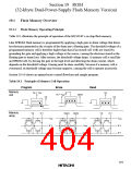
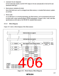
19.1.4 Block Diagram
Figure 19.1 shows a block diagram of the flash memory.
8
Internal data bus (upper)
8
Internal data bus (lower)
Operating
mode
MD1
MD0
Bus interface and control section
FLMCR
H'0000
H'0002
H'0004
H'0001
H'0003
H'0005
EBR1
EBR2
On-chip flash memory
(32 kbytes)
H'7FFC
H'7FFE
H'7FFD
H'7FFF
Upper byte
Lower byte
(even address)
(odd address)
Legend:
FLMCR: Flash memory control register
EBR1: Erase block register 1
EBR2: Erase block register 2
Figure 19.1 Flash Memory Block Diagram
377

 HITACHI [ HITACHI SEMICONDUCTOR ]