Section 19 ROM
(32-kbyte Dual-Power-Supply Flash Memory Version)
19.1
Flash Memory Overview
19.1.1 Flash Memory Operating Principle
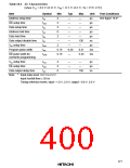
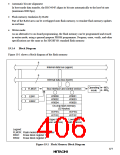
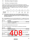
Table 19.1 illustrates the principle of operation of the H8/3434F’s on-chip flash memory.
Like EPROM, flash memory is programmed by applying a high gate-to-drain voltage that draws
hot electrons generated in the vicinity of the drain into a floating gate. The threshold voltage of a
programmed memory cell is therefore higher than that of an erased cell. Cells are erased by
grounding the gate and applying a high voltage to the source, causing the electrons stored in the
floating gate to tunnel out. After erasure, the threshold voltage drops. A memory cell is read like
an EPROM cell, by driving the gate to the high level and detecting the drain current, which
depends on the threshold voltage. Erasing must be done carefully, because if a memory cell is
overerased, its threshold voltage may become negative, causing the cell to operate incorrectly.
Section 19.4.6 shows an optimal erase control flowchart and sample program.
Table 19.1 Principle of Memory Cell Operation
Program
Erase
Read
Memory
cell
Vg = VPP
Vg
Vs = VPP
Open
Vd
Vd
Memory
array
Vd
0 V
Open
Open
Vd
0 V
VPP
0 V
0 V
0 V
VPP
0 V
VCC
0 V
0 V
375

 HITACHI [ HITACHI SEMICONDUCTOR ]