Bit 2—Output Compare Flag B (OCFB): This status flag is set to 1 when the FRC value
matches the OCRB value. This flag must be cleared by software. It is set by hardware, however,
and cannot be set by software.
Bit 2: OCFB
Description
0
To clear OCFB, the CPU must read OCFB after it has been set to 1, then write
a 0 in this bit.
(Initial value)
1
This bit is set to 1 when FRC = OCRB.
Bit 1—Timer Overflow Flag (OVF): This status flag is set to 1 when FRC overflows (changes
from H'FFFF to H'0000). This flag must be cleared by software. It is set by hardware, however,
and cannot be set by software.
Bit 1: OVF
Description
0
To clear OVF, the CPU must read OVF after it has been set to 1, then write a 0
in this bit.
(Initial value)
1
This bit is set to 1 when FRC changes from H'FFFF to H'0000.
Bit 0—Counter Clear A (CCLRA): This bit selects whether to clear FRC at compare-match A
(when the FRC and OCRA values match).
Bit 0: CCLRA
Description
0
1
The FRC is not cleared.
The FRC is cleared at compare-match A.
(Initial value)
8.2.6
Timer Control Register (TCR)
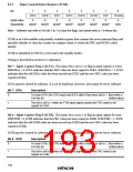
Bit
7
IEDGA
0
6
5
4
3
2
1
0
IEDGB IEDGC IEDGD BUFEA BUFEB
CKS1
0
CKS0
0
Initial value
Read/Write
0
0
0
0
0
R/W
R/W
R/W
R/W
R/W
R/W
R/W
R/W
TCR is an 8-bit readable/writable register that selects the rising or falling edge of the input capture
signals, enables the input capture buffer mode, and selects the FRC clock source.
TCR is initialized to H'00 by a reset and in the standby modes.
166

 HITACHI [ HITACHI SEMICONDUCTOR ]