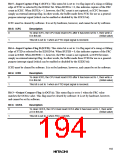
Bit 3—Output Enable A (OEA): This bit enables or disables output of the output compare A
signal (FTOA).
Bit 3: OEA
Description
0
1
Output compare A output is disabled.
Output compare A output is enabled.
(Initial value)
Bit 2—Output Enable B (OEB): This bit enables or disables output of the output compare B
signal (FTOB).
Bit 2: OEB
Description
0
1
Output compare B output is disabled.
Output compare B output is enabled.
(Initial value)
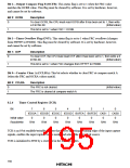
Bit 1—Output Level A (OLVLA): This bit selects the logic level to be output at the FTOA pin
when the FRC and OCRA values match.
Bit 1: OLVLA
Description
0
1
A 0 logic level is output for compare-match A.
A 1 logic level is output for compare-match A.
(Initial value)
Bit 0—Output Level B (OLVLB): This bit selects the logic level to be output at the FTOB pin
when the FRC and OCRB values match.
Bit 0: OLVLB
Description
0
1
A 0 logic level is output for compare-match B.
A 1 logic level is output for compare-match B.
(Initial value)
169

 HITACHI [ HITACHI SEMICONDUCTOR ]