Pin
Pin Functions and Selection Method
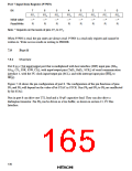
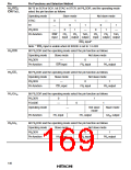
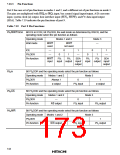
P84/IRQ3/
IOW/TxD1
Bit TE in SCR of SCI1, bit STAC in STCR, bit P84DDR, and the operating mode
select the pin function as follows
Operating mode
STAC
Slave mode
Not slave mode
0
1
—
0
TE
—
—
0
1
1
P84DDR
Pin function
0
1
—
0
1
—
IOW
input
P84
P84
TxD1
P84
P84
TxD1
input output output
input output output
IRQ3 input*
Note: * IRQ3 input is usable when bit IRQ3E is set to 1 in IER
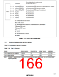
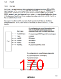
P83/IOR
P82/CS1
P81/GA20
Bit P83DDR and the operating mode select the pin function as follows
Operating mode
P83DDR
Slave mode
—
Not slave mode
0
1
Pin function
IOR input
P83 input
P83 output
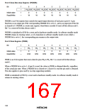
Bit P82DDR and the operating mode select the pin function as follows
Operating mode
P82DDR
Slave mode
—
Not slave mode
0
1
Pin function
CS1 input
P82 input
P82 output
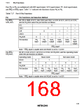
Bit P81DDR and the operating mode select the pin function as follows
P81DDR
0
1
FGA20E
—
0
1
Operating mode
—
Not slave
mode
Slave mode
GA20 output
Pin function
P81 input
P81 output
P80/HA0
Bit P80DDR and the operating mode select the pin function as follows
Operating mode
P80DDR
Slave mode
—
Not slave mode
0
1
Pin function
HA0 input
P80 input
P80 output
140

 HITACHI [ HITACHI SEMICONDUCTOR ]