7.10
Port 9
7.10.1 Overview
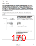
Port 9 is an 8-bit input/output port that is multiplexed with interrupt input pins (IRQ0 to IRQ2),
input/output pins for bus control signals (RD, WR, AS, WAIT), an input pin (ADTRG) for the
A/D converter, an output pin (ø) for the system clock, host interface (HIF) input pins (ECS2,
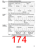
EIOW), and the I2C data input/output pin (SDA). Figure 7.17 shows the pin configuration of port
9. The functions of pins P91 and P90 are configured according to bit STAC in STCR. Pins P97 to
P92 are unaffected by bit STAC.
Pins in port 9 can drive one TTL load and a 90-pF capacitive load. They can also drive a
darlington transistor. Pin P97 can be driven as a bus buffer, as shown in section 13, I2C Bus
Interface.
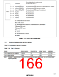
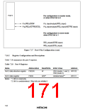
Pin configuration in mode 1 (expanded mode
with on-chip ROM disabled) and mode 2
Port 9 pins
(expanded mode with on-chip ROM enabled)
P97/WAIT/SDA
P96/ø
P97 (input/output)/WAIT (input)/SDA (input/output)
ø (output)
P95/AS
AS (output)
P94/WR
P93/RD
WR (output)
Port 9
RD (output)
P92/IRQ0
P92 (input/output)/IRQ0 (input)
Pin configuration in mode 3 (single-chip mode)
P97 (input/output)/SDA (input/output)
P96 (input)/ø (output)
P95 (input/output)
P94 (input/output)
P93 (input/output)
P92 (input/output)/IRQ0 (input)
Figure 7.17 Port 9 Pin Configuration
141

 HITACHI [ HITACHI SEMICONDUCTOR ]